关键词 > ECE2072
ECE2072 Project
发布时间:2025-10-17
Hello, dear friend, you can consult us at any time if you have any questions, add WeChat: daixieit
ECE2072 Project
Welcome and Getting Started
Welcome to the ECE2072 project, where you will be creating a processor that can run a set of given instructions. Your project to do so has been broken up into 4 main sections:
● Task 1: Create and test the building blocks required to make the processor
● Task 2: Create and test a processor that implements a handful of basic instructions
● Task 3: Extend your processor to implement extra, more complicated instructions.
● Task 4: Use instruction memory and a branch instruction to run programs.
● Report: Explain and justify the design decisions that were made during the creation of this processor
This document is long (although only 18 pages actually contain things you have to do). To get started with this project, we recommend you:
1. Read the first 5 pages of this document, which introduce the project and logistics
2. Do a ‘high level’ (skim) read through of the specification of the x72 processor first (on Moodle)
3. Do a ‘high level’ read through this document
4. Compare notes and understanding with your partner
5. Start attempting task 1
You should frequently come back to the detailed specification as required to ensure your design meets all of the requirements (this is to give you experience with implementing complex requirements).
At the bottom of the document, you will also find:
- A marking guide to walk you through how your project will be marked.
- A report guide to walk you through our expectations of your report.
- A FAQ section to answer any common questions that people have. This will be updated as time goes on to answer any recurring questions.
Introduction and Learning Outcomes
This project builds on the knowledge you have developed, and gives you an opportunity to demonstrate what you have learned around the digital design process. Your solution is expected to be written in high-level Verilog code and make use of Verilog language features that you have been introduced to in the labs. You will make use of and solidify your understanding of:
|
● Behavioural Verilog Code ● Finite State Machines ● Test Benches |
● Digital Logic Design ● Sequential Logic
|
You are also required to write a formal report that explains and justifies your design process and decisions.
We do not expect you to be familiar with processors, datapaths, or any related concepts. To get you up to speed, and introduce the way the x72 processor itself works, we have compiled a lesson about processors and datapaths for your convenience (on Moodle CL: here, MUM: here). Depending on your background, you may also need to do some independent reading about the basics of processors and datapaths (and cite your references) in order to fill in any gaps you may have, although this should not be necessary to complete the majority of the project.
Revision History
Use this revision history to monitor for any changes we may need to make to this document to clarify requirements or provide hints
|
Description |
Version |
Date |
|
Initial release |
1.1.0 |
02/09/2025 |
|
Updated link to processors and datapath moodle lesson |
1.1.1 |
08/09/2025 |
|
|
|
|
|
|
|
|
|
|
|
|
|
|
|
|
|
|
|
|
|
|
|
|
Key Information and Notices:
The HDL Style Guide you are expected to follow for this project is available in appendix B.
Estimated Time Commitment: ~15-20 hours each for a Credit. A fully working solution and report will take considerably more time than this.
Groups:
The ECE2072 project is to be completed in pairs. You can nominate your preferred partner. If you do not nominate your preferred partner by the end of week 7, you will be assigned one. You may nominate someone from a different lab (subject to capacity), but you both must be able to attend the same lab session for marking in week 12.
If you wish to make alternate arrangements, please reach out to the teaching team.
Academic Integrity
You may discuss general details (eg: approaches) of the project with other students. However, you may not:
● write the code together with students from other groups,
● show student from other groups your HDL,
● copy other group's work, or
● present work you have found online as your own (i.e. without attribution),
This is plagiarism and/or collusion and is prohibited by Monash’s academic integrity policy. Breaches of this policy attract serious consequences. Note that all code submitted to this unit will be run through the MOSS system to check for plagiarism.
If you research some concept online or re-use HDL from your labs (or from this unit) you must cite it (any citation method is acceptable).
Generative AI:
As a reminder, you can use generative artificial intelligence (AI) in order to troubleshoot your solutions, explain concepts and assist you in preparing your reports.
Both students in a group must fully understand the work submitted for assessment - if you do not understand your work, you may receive a zero interview score, which will result in a zero for the project.
Any use of generative AI for this purpose must be appropriately acknowledged, if you do not acknowledge your use of AI, it may be submitted as plagiarism under the academic integrity guidelines. You must not use generative artificial intelligence (AI) to generate any HDL for submission.
Submission, Presentation & Marking
Design Due: Friday, 17th October, 11:55 PM (End of Week 11)
Presentation: Assigned time slot in scheduled lab session (Week 12)
Report Due: Friday, 24th October, 11:55 PM (End of Week 12)
Submission File Structure:
You are required to submit your entire Quartus project on Moodle, along with a 1 page ‘work summary’ document, describing which parts of task 1 you’ve each done, and both of your overall contributions to the project, which we will use to have a discussion about scaling your individual scores if required. You can do this by archiving the project file via Quartus. A checklist is provided here.
We will be marking your functionality by importing your Quartus Archive, and compiling it on the lab machines. Mark penalties will apply if your marker has to debug your design.
Therefore, ensure you have tested your project submission by re-downloading your .qar file (after you have placed it on Moodle) and testing it for functionality BEFORE clicking submit. Ensure all relevant files are present in your .qar’s file directory.
We will mark you on your choice of device (DE2-115/DE10).
You must submit your formal report in PDF format. You will be provided with a google drive folder for your team, which should include all ‘artefacts’ (i.e. documentation, test benches, outputs) you need to support your report. You should hyperlink from your report to the appropriate document you wish to reference to support your work (think of it like a searchable appendix). Testbench artefacts should be properly exported as per the instructions in Lab 2.
Late Submissions:
The design and the report are separate submissions. Late submissions will only be accepted until your lab class unless special consideration is granted. The standard (5%) penalty applies for every late day.
Special Consideration:
For extensions, you must apply through Monash Special Consideration. The report is a separate assessment and must be extended separately. Note if you receive an extension until after your scheduled lab class, you will need to attend an alternative session to demonstrate your work. You must still demonstrate your work in person with your partner.
Mark Distribution:
The 10% of the final project grade is broken down between the design task (7%) and the report (3%), with the whole project scaled by an individual interview. A detailed mark distribution is included at the end of the project, and a rubric will be linked from this section.
Completing tasks 1 and 2, coupled with a ~credit level report, will get a credit overall.
Background Overview
The following is an abridged version of the background information supplied in the processors and datapath moodle lesson, which introduces this architecture. We will refer back to this lesson for key details throughout this document.
A computer processor, also known as a central processing unit (CPU), is a sequential digital circuit that performs the calculations that make a computer ‘run’. It performs arithmetic and logical operations, input/output (I/O), and other basic instructions. In this project, you will be making your own processor, which we are calling an ‘x72’. You will begin by creating a simple processor, and progressively add additional features and functionalities.
A simple processor has several individual components that all work together to perform operations, the x72 processor that is designed in the project is shown in the image below.
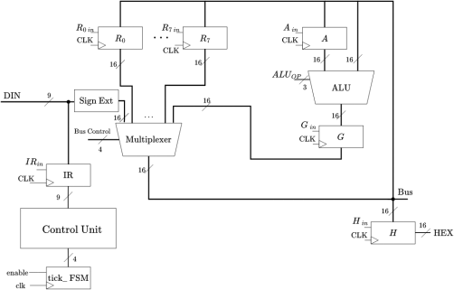
Task 1: The CPU Components
To begin, we must first create each of the building blocks (components) we will use to make our processor. Using the provided skeleton file named components.v, write Verilog HDL to implement each of the 5 component modules we require to construct the simple CPU.
The specifications for the components you are required to create are described below. Note that you do not need to implement the control unit in task 1. You are welcome to extend upon the building blocks you developed in Lab 2 to complete this task.
The design and implementation of these modules must be split between both members of your group. Each student will receive a score for task 1 based only on the functionality of the components they designed. This split must be formally documented in both your HDL (via comments) and in your report.
Note, you are each still required to completely understand the functionality of all components. This is important as they will be needed in every subsequent part of the project. You may be asked questions about any of these components during your interview.
1 - Sign extender:
You may have noticed that a 9 bit DIN input wire doesn’t have the same width as our 16-bit data bus. You should write a sign extender module to deal with this issue. When a 9-bit word is inputted to this module, the output should be the corresponding sign-extended 16-bit binary number. To sign-extend, you need to pad the most significant bits [15:9] with a ‘1’ if the input number is negative, and a ‘0’ if positive. You should try this by hand to make sure that your module works for both positive and negative 2s complement number
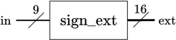
Figure 1: A high-level diagram of the sign extension module.
2 - Tick Counter:
Design and write a Tick finite state machine to maintain the current state of the processor. Your FSM must meet the following specifications. It should have three input (an enable, a reset, and a clock), and a 4 bit output to represent the 4 possible ticks of the system. When enable is asserted, the output should cycle through a state representing each of the four ticks described in the section “detailed breakdown of instructions” in the x72 lesson in Moodle. Click here instead for Malaysia campus
Your FSM must make use of one-hot coding, and use the minimum number of both registers and states to implement the required functionality, given this constraint.
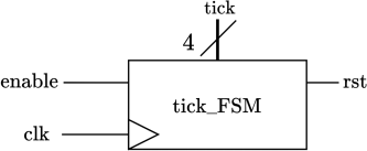
Figure 2: A high-level diagram of the tick_FSM module
In components.v, write a module tick_FSM that implements the FSM described above. A skeleton has been provided for you in the skeleton code in components.v. Note that you must not change the names of the input and output ports for the tick_FSM module (these need to match the image shown in Figure 2).
3 - The ALU:
The ALU module, as shown in figure 3 below, has three inputs and one output. The ALU performs operations on the two 16-bit inputs input_a and input_b, based on the select input of alu_op.
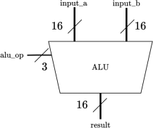
Figure 3: A high-level diagram of the ALU module
The operation to perform corresponding to the alu_op input is summarised in table 3 below.
Table 3: ALU operation summary.
input_a comes from register A, input_b comes from the bus wires
|
alu_op |
Operation |
|
000 |
input_a * input_b (multiplication) |
|
001 |
input_a + input_b (addition) |
|
010 |
input_a - input_b (subtraction) |
|
011 |
input_b shifted by input_a (signed shift) |
|
100 |
None (don’t care) |
|
101 |
None (don’t care) |
|
110 |
None (don’t care) |
|
111 |
None (don’t care) |
In components.v, write an ALU module named alu that implements the logic described above. A skeleton has been provided for you in the skeleton code in components.v. Note that you must not change the names of the input and output ports for the alu module.
4 - The Multiplexer:
The multiplexer module, as shown in Figure 4 below, is how the bus of the processor is implemented. It has ten 16-bit data inputs - for registers 0-7, register G, and the sign extended version of the 9-bit data input (DIN). It has a 4-bit input select line that controls which data input appears on the output.
The output of the MUX will be used to feed into registers 0 through 7, register A, register H, and the ALU. The values on the bus wires will only be stored into a register when the enable signal on that register is asserted.
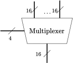
Figure 4: A high-level diagram of the multiplexer module
5 - Registers:
The register module, as shown in figure 5 below, has four inputs and one output. On the rising edge of the clk input and if the rst input is asserted, then the register contents is reset to 0. Otherwise, if the r_in enable input is asserted, then the data on the data input, data_in, is stored in the register. The data output, Q, is the value that is currently stored in the register.
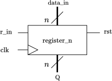
Figure 5: A high-level diagram of the register module
In components.v, write a register module named register_n that implements the logic above. Your design should use a parameter n that allows the number of bits that the register stores to be changed across instantiations as the instruction register and general purpose register holds different numbers of bits. A skeleton has been provided for you in the skeleton code for components.v. Note that you must not change the names of the input and output ports for the register_n module.
Testbench:
After implementing each of the components above, write a testbench in a file named components_tb.v that implements a process to intelligently test each of the modules you have created. A skeleton has been provided for you in the skeleton code for components_tb.v.
Each student must claim responsibility, via HDL comments and the ‘work summary’ document for at least two of these test cases, the total number of test cases, and the work distribution is a choice for you to justify as a pair.
You will be assessed (in the live demonstration and report) on whether:
● The testbench checks each component
● The testbench intelligently checks all functions of each component
● The testbench reports clearly that a component has passed
● The testbench report clearly shows what tests have failed in a manner that would aid debugging
○ If you do have failed tests, you will receive more marks for having the testbench clearly documented rather than trying to hide them
● A summary of the results is clearly printed at the conclusion of the testbench
Task 2: The simple processor
In this task, you will implement the x72 processor architecture using your components from Task 1. For now, you will only be implementing a subset of the total processor. A simplified diagram containing only the aspects of this task are shown below:
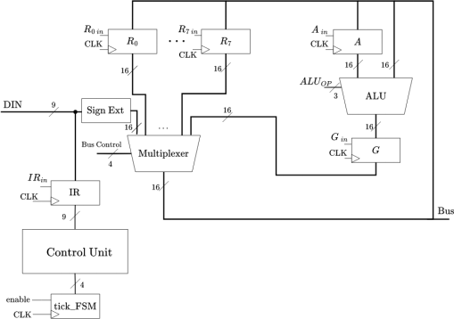
Figure 6: An internal diagram of the task 2 processor
You will implement the processor in a module named simple_proc. A skeleton has been provided for you in the skeleton code for proc.v. Note that you must not change the names of the input and output ports for the simple_proc module.
Note: The skeleton you are provided with includes output ports to output the values of the internal registers R0 - R7, for the purpose of test benching. When instantiating the processor to program your DE10-lite, you can leave these ports unused.
Your simple processor must support the following instructions (using the instruction encoding specified in the x72 lesson):
● Move immediate (movi)
● Addition (add)
● Add Immediate (addi)
● Subtraction (sub)
Testing your Implementation
Important: Functional marks for task 2 are for demonstrating that your system works. To do this, you must use a mixture of hardware and simulation. Your demonstration time is limited, and how you use it is part of the assessment. Therefore, note you will not be able to achieve full marks by trying to demonstrate full functionality via extended hardware simulation of many instructions (for hopefully obvious reasons).
Hardware in Loop Testing
To test with the DE10 (or DE2), write a top-level module which does the following:
● Instantiates the processor module
● Connects SW[8:0] to the bus input of the processor
● Connects ~KEY[0] to the reset input of the processor, to use as a synchronous reset
● Connects a 1’b1 to the enable input of the tick_FSM, to permanently ‘lock’ the processor into its ON state for this phase of the project
● Connects ~KEY[1] to the clock input of the processor
● Connects LEDR[9:0] to the bottom 10 bits of the bus output of the processor
● Decodes the tick_FSM output of the processor into a 7-seg format (e.g., using modified BCD) and displays the current tick on HEX5[6:0]
A block diagram of your top-level Verilog module should match this diagram:
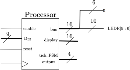
Figure 7: A block diagram of the top level module for task 2
You can then test that your processor works correctly by setting SW[8:0] to an encoded instruction, and pressing KEY[0] to pulse the clock. You can observe the values appearing on the bus (LEDR) to confirm the processor is behaving as expected.
Simulation Testing
Hardware testing is critical, but this is limited, and doesn’t let us test multiple instructions or verify things easily. To fully test our processor, we will need to use a testbench.
In a file named proc_tb.v, write a testbench that instantiates the processor and simulates the execution of the specified instructions. You can view the waveform of the internal processor registers/wires to verify that your processor is correct, however this will not let you effectively test/prove accuracy of the instructions. Therefore, you must include print statements for your testbench.
For full marks, you must clearly demonstrate that your design meets the specifications of task 2. How you set up your “test campaign” to do this (i.e., the test benches you run) is part of the project, but must contain a mix of hardware and simulation results.
More specifically, you will be assessed (in your demonstration and report) on:
● What combination of cases and/or selection method you choose to use for your tests.
● The clarity and presentation of the reporting of your testbenches. This includes how you report errors/failed tests, even if they are not triggered.
● How you decide to operate your tests (ie: assumptions and configurations).
● Your justification of why your test cases are sufficient to prove correct operation.
There is no “one correct answer” to this problem. This is representative of many real world engineering scenarios you will run into as the years go by, so we believe it’s important you get used to working with this type of open-ended challenge early in your degree.
Task 3: Adding an Output Peripheral and New Instructions
In this task, you will be adding an output peripheral to your processor in the form of a hex display. In a file named proc_extension.v, copy in the code from task 2 and modify the processor module to include a new output port named display, and support a disp Rx instruction, which should output the value of Rx to this new output display port.
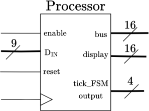
Figure 8: A high level diagram of the processor with a display output
Any value written to the display port should remain displayed while other instructions are executing, until the next display instruction is executed.
You can implement the display instruction by modifying the internal processor to include a new 16-bit ‘display’ register (also referred to as register H in the x72 architecture) that is connected to the output, and modifying the control unit to assert the displayin control signal when the desired display value is output onto the bus.
Additionally, you will be adding support for the following instructions (using the instruction encoding specified in the x72 lesson):
● Signed-shift-immediate (ssi)
● Multiplication (mult)
● Display (disp)
Testing your Implementation
Important: Functional marks for task 3 are for demonstrating that your system works. It is up to you to decide how to do this. Your demonstration time is limited, and how you use it is part of the assessment. We recommend selecting a mixture of hardware demos and simulation results that demonstrate the extensions to your processor (on top of the functionality in task 2) work as intended.
Hardware Testing
Once you have implemented the changes to your processor, write a top-level module that does the following:
● Instantiates the processor module
● Connects SW[9] to the enable input of the processor
● Connects SW[8:0] to the DIN input of the processor
● Connects ~KEY[0] to the reset input of the processor, to use as a synchronous reset
● Connects ~KEY[1] to the clock input of the processor
● Connects LEDR[9:0] to the bottom 10 bits of the bus output of the processor
● Uses a BCD decoder to decode the display output of the processor to HEX4 to HEX0 as an signed 16-bit integer.
● Decodes the tick_FSM output of the processor into a 7-seg format (e.g., using modified BCD) and displays the current tick on HEX5[6:0]
Your top-level module should look like the following:
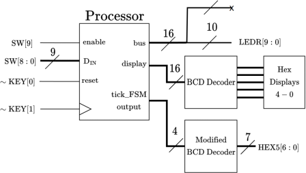
Figure 9: A block diagram of the top level module for task 3. Note we only want to extract the lower 10 bits from the register for the LEDR output.
Task 4: Instruction Memory and Branching
In this task, you will be interfacing your processor with some instruction memory made with a read-only memory (ROM) Quartus IP block, and extending your processor such that it is Turing complete.
This task is designed to be an extension for the students aiming for high-HD marks (85+%). We have not provided you with a template datapath to use. You may need to make several adjustments/additions to other components in your processor to successfully accomplish this task (new ALU instructions, extending the ticks per instruction etc).
Instruction Memory:
In a file called ‘proc_memory’, copy your Verilog from task 3, and add the program counter (PC) register to your processor's datapath to track where in memory your processor will take its next instruction from.
Next, create an instance of the Quartus ROM IP block that will be used as your instruction memory. Each word should be the same width as Din, and the block’s size should represent the total amount of instructions that could be addressed by a 16-bit address. You should assume all instructions use 2 words for ease of use. See Appendix C for instructions on how to pre-program the ROM with assembly code.
In order to interface with the ROM IP block, your processor will need to export the current 16-bit program counter value from the new ‘PC’ output wires. This will then act as the address read in by the instruction memory, which will feed the requested instruction into the Din of your processor. At the end of each instruction, you will perform a ‘+2’ operation on the value in the program counter (1 for the instruction, 1 for the immediate), so that the next instruction may be read in.
For immediate instructions, you would add 1 to the PC to retrieve the immediate value, then add 1 again for the next instruction.
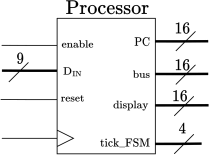
Figure 10: A block diagram for the processor module in task 4.
Branching:
Finally, you will add support for the bez Rx imm instruction which will adjust the current program counter value based on the value in Rx and the immediate provided (as specified in the x72 lesson in Moodle). You may assume that whoever wrote the assembly has correctly encoded the instruction such that the value received contains the appropriate adjustments to the immediate value such that it represents the number of instructions that the PC will jump by. I.e. bez 0, 6 is a 6-instruction jump.
Testing your Implementation
Once you have implemented the changes to your processor, write a top-level module that does the following (note, a testbench is not required for task 4):
● Instantiates the processor module (as specified in the x72 lesson)
● Instantiates the instruction memory as your ROM IP-block (See programming instructions in Appendix C)
● Connects the input address of the instruction memory to the processor's PC output.
● Connects the output of the instruction memory to the Din input of the processor
● Connects SW[9] to the enable input of the processor, so we can pause the program.
● Connects ~KEY[0] to the reset input such that we can fully reset the processor.
● Connects the clock input of the processor to a 10 Hz clock (see Lab 3 for instructions on making this yourself.)
● Connects LEDR[9:0] to the bottom 10 bits of the bus output of the processor
● Uses a BCD decoder to decode the display output of the processor to HEX4 to HEX0 as an unsigned 16-bit integer.
● Decodes the tick_FSM output of the processor into a 7-seg format (e.g., using modified BCD) and displays the current tick on HEX5[6:0]
Your top-level module should look like the following:
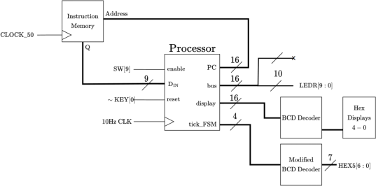
Figure 11: A block diagram of the top level module for task 4.
Reporting
We are expecting you to submit a formal design report, of approximately 6-8 pages (roughly 2500 words) not including references or appendices. Your report should contain:
● A brief introduction to what you were asked to do, and your design, assuming the person reading your report is not familiar with the x72 architecture or this document, but has completed ECE2072.
● An overview of each component you have implemented in task 1, highlighting any design choices you have made, the functionality of the components, and a summary of resource usage and maximum frequency of each component (timing analysis).
● A detailed description of how your implemented datapath executes two instructions (one after the other) of your choice. Choose your instructions to best illustrate the functionality you have achieved (if you have only done task 2, do ones from task 2)
● A detailed discussion of the design of your testing regime for all tasks (at least 3 pages), including summarised key results (including waveform excerpts if appropriate) from the testbenches.
● A conclusion, summarising your justification that your design is functional and fit for deployment.
We realise that 6-8 pages isn’t a huge amount of space for this much information! Part of writing well technically is learning how to be concise, which is also part of your challenge with this project.
Going over this amount of pages/words will not result in mark deductions provided you have good reason to do so. If you could have been more concise, you will lose marks. Playing around with formatting to ‘squeeze in’ more text will not make your report clearer, and so will also most likely attract a deduction.
You can find further details on the standards and requirements of technical reports from the Monash Report Standards site.