关键词 > EECS31L
EECS31L Introduction to Digital Logic Design Lab Winter 2025 Lab 4
发布时间:2025-03-08
Hello, dear friend, you can consult us at any time if you have any questions, add WeChat: daixieit
Introduction to Digital Logic Design Lab
EECS31L
Winter 2025
Lab 4 (100 Points)
Through this course, we want to design a RISC-V Single Cycle Processor. Here in this Lab, we will work on the Datapath part of the processor. In Part 1, we again review the RISC-V datapath. In part 2 we talk about how to design the data memory and in part 3 we talk about designing the datapath and finally in part 4 we test the datapath.
1 Datapath
Figure 1: RISC-V Datapath.
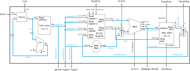
Figure 1 shows the datapath of a RISC-V single cycle processor. The instruction execution starts by using the program counter to supply the instruction address to the instruction memory. After the in- structionis fetched, the register operands used by an instruction are specified by fields of that instruction. Once the register operands have been fetched, they can be operated on to compute a memory address (for a load or store), to compute an arithmetic result (for an integer arithmetic-logical instruction), or an equality check (for a branch). If the instruction is an arithmetic-logical instruction, the result from the ALU must be written to a register. If the operation is a load or store, the ALU result is used as an address to either store a value from the registers or load a value from memory into the registers. The result from the ALU or memory is written back into the register file. The blue lines interconnecting the functional units represent buses, which consist of multiple signals. The arrows are used to guide the reader in knowing how the information flows. Since signal lines may cross, we explicitly show when crossing lines are connected by the presence of a dot where the lines cross.
Some of the inputs (RegWrite, ALUSrc, ALUCC, MemRead, MemWrite, MemtoReg) are control signals which are derived by a module named “Control” . The control unit will be designed in Lab 5. Here in this lab, assume you have all the control signals as inputs.
Table 1 shows the list of Instructions that our Datapath supports.
Table 1 : Instruction Set.
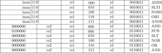
Note: along with the provided instructions in Table 1, your datapath needs to support "lw" and "sw" instructions too. Table 2 and 3 show format of these two data-transfer instructions.
Table 2 : Instruction Set (lw).

Table 3 : Instruction Set (sw).

For this part, you need to save these two instructions into the ”Instruction Memory” that you designed in lab 3. Add the following two instructions into the instruction memory (as you did in lab 3):
memory[18] = 32’h02b02823; // sw r11, 48(r0) alu result = 32’h00000030
memory[19] = 32’h03002603; // lw r12, 48(r0) alu result = 32’h00000030 , r12 = 32’h00000005
2 Lower Level Modules
As it is shown in Figure 1, there is a top module (Datapath) and nine lower-level modules (FlipFlop, Adder, Instr mem, RegFile, Imm Gen, Mux (two instantiations), ALU, data mem). Eight sub-modules are designed in the previous labs and in this lab, we start by designing the last sub-module which is data mem.
Note: 32-bit ALU design source is provided for you in section 2.2. You are welcome to use your own design source from Lab 2, if your design source got the full point.
2.1 Data Memory
Same as the Instruction Memory (refer to the previous lab), the Data Memory in our processor is byte addressable. We can store 128 data each with 32 bits (128 x 32). To address 128 x 4 = 512 bytes, 9 bits are required for address line. These 9-bits come from the 9 LSBs of the output of the ALU (ALU Result). To read a data, we need an address (addr[8:2] which uses bit 2 to bit 8 from 9-bit addr) and the read enable signal (MemRead). To write a data, we need an address (addr[8:2] which uses bit 2 to bit 8 from 9-bit addr), the write enable signal (MemWrite), and a data to write (write data).
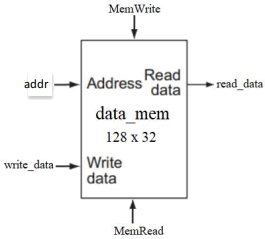
Note: Use the provided module definition to design your Data Memory. Otherwise, your submission will not be considered for grading.
Code 1: Data Memory
2.2 Mux
The MUX on the output of the Data Memory will decide whether the writing data (to the register file) should come from the ALU or come from the Data Memory (refer to Figure 1). You can use 2-to-1 Mux design from Lab 1. The only diference is that for this datapath, you need to consider size of input data and output data for each 2-to-1 Mux. For example, for the last 2-to-1 Mux in datapath (refer to Figure 1), size of data input is 32 bits. Follow the same rule for the Mux which is before ALU in the datapath.
2.3 32-bit ALU
Code 2: 32-bit ALU
2.4 Adder
You can directly use the addition operator in Verilog ‘+ ’ to calculate the next pc (PCPlus4 in Figure 1). Don’t use a separate adder module to calculate PCPlus4.
3 Higher Level Module
Now that we have designed all of the submodules, we can use them as a component and design the Datapath. Here again, you see the Datapath. Blue lines are wires used to connect the submodules. Define these blue lines as “wire” and connect the components to complete the Datapath.
Use the following code for the module definition of your Datapath.
For Datapath code, we used lowercase letters for input/output naming. You need to use the exact code samples provided for you to design the Datapath and tb Datapath. Otherwise, your submission will not be considered for grading.
Careful! * The port names in the diagram are slightly diferent than the port names in the module definition. When writing your code, please use the port names provided in the module definition. (The diagram is just provided for visual purposes.).
*Pay attention to the orientation of MUX in the figure (which signals are passed to D0 & D1)
*PC increments by 4 bytes to get the next instruction because RISC-V uses byte-addressable memory.
Code 3: Datapath
Important Note: we want you to have separate source files for each of the datapath sub- modules.
4 Test the Datapath
Use the code bellow to test your Datapath design.
Code 4: tb Datapath
44
45 /** Stimulus **/
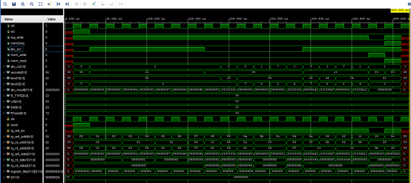
Check the outputs (opcode, funct3, funct7, alu result) to see if they are correct. Put a screenshot of the wave in your report. Here you see the screenshot of the wave for the datapath:
Note1: After running the simulation, you can add modules/signals from the scope tab to add more signals. After adding the signal to the wave window you re-run the simulation to show the updated values.
Note2: For Windows users, the use of the slicing operator on the ‘instruction’ wire to pass values to the register file input ports ‘rg rd addr1’ , ‘rg rd addr2’ and ‘rg wrt addr’ - as shown below - might result in a faulty output waveform:
Code 5: Problematic Register File Instance
Although this issue will not afect the correctness of the module’s functionality, it can be avoided by creating wires and assigning them to the sliced values and finally connecting these new wires to the ports of the register file as follows:
Code 6: Solution
5 Assignment Deliverable
Your submission should include the following:
• Block designs and testbenches. (FlipFlop.v, InstMem.v, RegFile.v, ImmGen.v, Mux.v, ALU.v, DataMem.v, Datapath.v. tb Datapath.v). Use the files we provided for you with this lab.
• For the Mux design, consider size of data inputs and change your previous designs to match with the processor datapath (see Figure 1).
• A report in pdf format. Follow the rules in the “sample report” .
Note1: Compress all files (10 files : 9 .v files + report.pdf) into zip and upload to the CANVAS before deadline. Make sure that you submit one .zip file, otherwise your submission will not be considered for grading.
Note2: Use the code samples that are given in the lab description. The module part of your code should exactly look like the code sample otherwise your submission will not be considered for grading.