关键词 > VHDL代写
ASSIGN Q5
发布时间:2024-06-19
Hello, dear friend, you can consult us at any time if you have any questions, add WeChat: daixieit
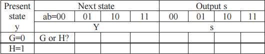
5) Figure 5a shows the block diagram of a serial adder. The serial adder adds two 8bit unsigned number A and B and produces the sum in the Sum-register. The heart of the serial adder is an Adder Finite State Machine (FSM) as shown in Figure 5b. The state of the FSM is the carry-in from the previous bit position, and it is denoted by G=0 or H=1.
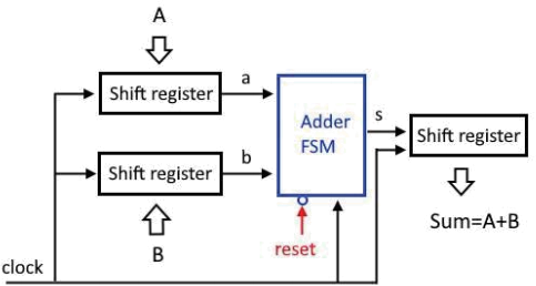
Figure 5a: Block diagram for the serial adder.

Figure 5b: Circuit for the adder FSM.
a) Complete the table below for the state transition and the output sum.
 (4 marks)
b) Write a VHDL code to implement the adder FSM, according to the table above. Explain the logic and algorithm by meaningful and explanatory comments in the code. Capture the screenshot of the source code in the Vivado software environment. (6 marks)
c) Synthesize and implement the design. Capture the screenshots of the schematic diagram produced by Vivado. You may combine b) and c) in one screenshot. (2 marks)
d) Write a test bench code to simulate the circuit function. In the test bench code, a clock signal shifts two 8bit unsigned numbers, A = a7a6 ... a0 and B = b7b6 ... b0 to the right bit by bit into the Adder FSM and shifts the output s into the sum-register. Capture the screenshot of the test bench code in the Vivado development environment. (4 marks)
e) With A = 00111011b and B=01011100b, run the simulation to obtain the sum s. Capture the screenshot of the simulation result. Compare with the result with the binary addition, and show whether the simulation result is correct. (6 marks)