关键词 > VE311
VE311 Electronic Circuit Homework 1
发布时间:2024-05-27
Hello, dear friend, you can consult us at any time if you have any questions, add WeChat: daixieit
VE311 Electronic Circuit Homework 1
Due: May 28th
Note:
1) Please use A4 size paper or page.
2) Please clearly state out your final result for each question.
3) Please attach the screenshot of Pspice simulation result if necessary.
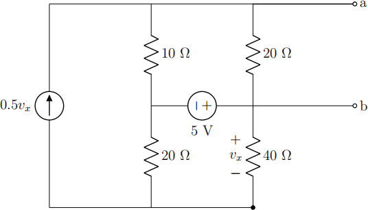
As a fan of photography, you decided to make your own camera based on knowledge you learned form VE311. Firstly, you have to obtain the desired voltage. Having built a circuit, please simplify it to verify the voltage between terminals.
Question 1. Thevenin Circuit
Obtain the Thevenin equivalent circuit at terminals a-b for the circuit below.
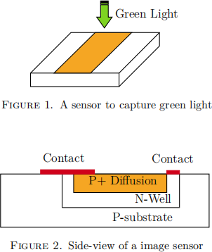
![]() After that, the image sensor drew your attention. To make it more sensitive to lights, you looked into its structure to fully understand the imaging principle
After that, the image sensor drew your attention. To make it more sensitive to lights, you looked into its structure to fully understand the imaging principle
Question 2. CMOS Image Sensors (CIS)
Consider the structure shown below where green light is only incident on the gate area and the rest of the area is shielded. Assume that the quantum efficiency is 30 %, which means only 30 out of 100 incident photons excite an electron-hole pair (An imaging-specific process nowadays typically have a quantum efficiency of 75%). The wavelength of green light λ = 550 nm. The size of the active area (Yellow area) W = L = 10 µm. You looked into textbook and found h = 6.626 × 10⁻³⁴ J·s.
(a) The CMOS camera is a PN junction. To understand how it works, you decide to revisit device physics. Consider a p-n diode with an abrupt junction. Assume that the doping densities on the p and n side are uniform and they are NA = 1019 /cm3 and ND = 1021 /cm3 respectively. Calculate the majority and minority carrier density in each side at thermal equilibrium. Assume that the intrinsic carrier concentration (free electron and hole carrier concentration of pure silicon) ni = 1.5 × 10¹⁰ /cm3 at room-temperature of 25 。C.
(b) For a CMOS camera to operate properly, you will have to set the bias condition of the photodiode. For a forward bias voltage of Vd = 0V , Vd = 0.5V and a reverse bias voltage of Vd = −1.7V , calculate the built-in potential (φ0 ) (Vd = 0V) and the potential barrier under the different bias conditions.
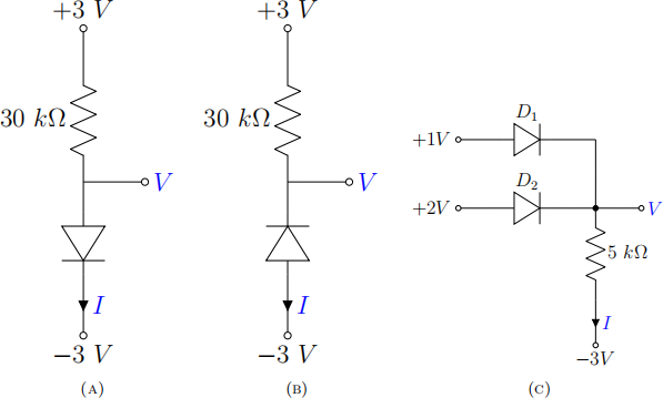
To connect different subsystems, you designed some diode circuits and analyzed them to see if they meet your requirements. To make your life easier, ideal diodes are assumed.
”Error is gonna be within 5% and be ignored.”you said to yourself.
Question 3. Diode Circuit Exercise 1
For each circuit below, assuming ideal diode model, calculate the labeled voltages and currents (V and I):
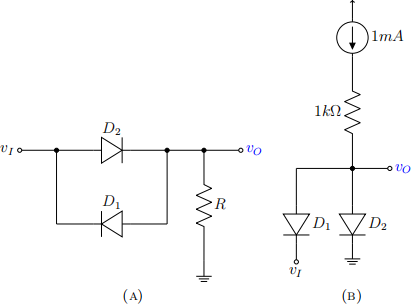
Question 4. Diode Circuit Exercise 2
In each of the ideal-diode circuits shown below, vI is a 1 kHz, 1 V peak sine wave with 0 initial phase. Sketch the output waveform vO as a function of time, showing the important values, such as the peak voltage values (positive and negative).
Unfortunately, however, unexpected errors showed up. You re-analyzed some crucial parts of your circuits using constant voltage drop model to see if any modifications are needed.
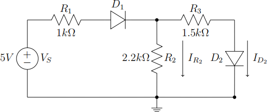
Question 5. Diode Circuit Exercise 3
In the circuit below, assume the constant voltage drop model for the diodes and assume the turn-on voltage is 0.7V. Calculate the values for current IR2 and ID2 .
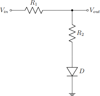
Question 6. Diode Circuit Exercise 4
Plot the input/output characteristics of the circuit below using the CVD model. Label critical points and slopes clearly.
After building the perfect circuit, you find that the signal does not have the desired wave form. To fix that, you apply some rectifiers to regulate your current signals.
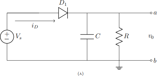
Question 7. Half-Wave Rectifier
You designed a half-wave rectifier circuit, such as below, which can convert a sinusoidal voltage input, Vs = 5sin(2π · 100 · t), to an almost constant voltage output.
(a) Assuming Von = 1.0 V and R = 100Ω, calculate C which makes the ripple voltage Vr is smaller than 0.1 V. Estimate Vdc ,Idc ,θc , ∆T,Ipeak , Isurge and PIV of the designed half-wave rectifier.
(b) Plot Vs and Voutversus time on the sample graph.
You are still not satisfied with the voltage wave form and want to obtain a more stable signal. Thus, you applied the knowledge on full wave rectifier you learned in Ve311 and designed a more advanced circuit.
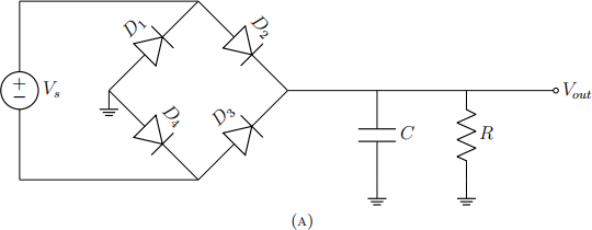
Question 8. Full-Wave Rectifier
You designed a full-wave bridge rectifier circuit, such as below, which can convert a sinusoidal voltage input, Vs = 5sin(2π · 100 · t), to an almost constant voltage output.
(a) Assuming Von = 1.0 V and R = 100Ω, calculate C which makes the ripple voltage Vr smaller than 0.1 V. Estimate Vdc ,Idc ,θc , ∆T,Ipeak , Isurge and PIV of the designed full-wave bridge rectifier.
(b) Plot Vs (using ”voltage differential marker” function) and Vout versus time on the sample graph.
![]()