关键词 > ELEC372/472
ELEC372/472: Integrated Circuit Design Assignment 1
发布时间:2023-11-27
Hello, dear friend, you can consult us at any time if you have any questions, add WeChat: daixieit
ELEC372/472: Integrated Circuit Design Assignment 1
Objectives:
. Understand the fundamental theory underlying internal and external capacitances of a MOSFET and simple CMOS inverter, and their effects on circuit performance as covered in ELEC372/472 in the context of design.
. Carry out basic calculations of such capacitances for a simple CMOS inverter so as to determine the value of the effective load capacitance. In later assignments, this load capacitance will be utilised in circuit simulations on a software package Multisim, to investigate how changes in device geometry affects the performance of CMOS-based circuits.
For guidance, a 15-credit module unit is meant to occupy 150 hours in total (including both private study and contact hours). You should aim to spend about 3-4 hours per week at the terminals. The remainder of the time will betaken up with background reading and research.
KEEP A LOG BOOK OF YOUR PROGRESS.
|
EFFECTIVE TIME MANAGEMENT IS A KEY SKILL THAT APPLIES TO ALL
PROFESSIONS AND WORKING SITUATIONS. SO IF YOU GET STUCK, ASK - DO NOT WASTE TIME - STAY FOCUSED |
Introduction
This task requires you to write a simple programme to perform basic calculations on inverter speed, as defined by fall-time. Fall-time is the time taken for ann-channel MOSFET in a CMOS inverter to pull-down the output from 90% to 10% of the supply voltage. The theory is presented in the lecture notes and further instructions are provided in appendix A.
Such "ball-park" or "back of the envelope" calculations are essential when performing simulation tasks, as there is a need to cross-check the numbers obtained from complex simulations are reasonable. The values you obtain from your simple model will also inform you on how to set-up your simulations, i.e. establish the time frame of interest and allow you to set the frequency of the test signals so as to correctly observe all the anomalies on the voltage-time plots etc. Furthermore, if you set a very long time frame, you may overload your memory store on the server. This approach should be applied in all your simulation assignments.
Instructions
Write a simple model in Matlab, C, python or anything else you prefer.
You should think about which parameters to define as variables and constants; certainly the transistor width (W) needs to be defined as a variable (see below). Make sure you use sensible values for a 1.2 μm technology as used in this course. In this case, the long-channel theory applies (explain why in your report), and for the CMOS design, assume an n-well process.
To develop the model for the effective load capacitor (CL) refer to the lecture notes and instructions below. Tables 1 and 2 provide a summary of the SPICE models and values for the 1.2 µm technology that you will utilise within the Multisim environment. Use these values in your calculations. A more detailed SPICE model will be provided in later assignment, and you will be able to compare your calculated values. When using the values in Table 2, take great care with the units since values in SPICE are not always quoted in SI units. Also check that the values you obtain for the parameters are sensible e.g., what value do you expect for the built-in voltage of ap-n junction?
Once your simple (I continue to emphasise its simple - don't look for complications!) programme is running and yielding sensible values, plot graphs of the following:
1. Fall time as a function of width, W – sensible range of values – you can not drive many gates at high speed;
2. Fall time as a function of fan-out (i.e. attach an increasing number of inverters to the test inverter); choose one value of W.
Submission
Download the Assignment 1 submission form on Canvas and fill-in all the sections below:
a) Provide basic description of the task. You can refer to the lecture notes for details of the derivation
b) Write a little on the APPROXIMATIONS assumed in that analysis.
c) Results/Graph and Comments from your programme for Fall time as a function of width. d) Results Graph and Comments from your programme for Fall time as a function of fan-out. e) Paste your source code.
Appendix A: Further instructions
How to estimate the load capacitance, CL
Figure 1 shows a CMOS inverter loaded with another inverter, also known as a unity fan-out inverter. The circuit displays respective key internal device capacitances that affect the output node (Vout). In order to estimate the switching time of such a circuit using the transient model derived in ELEC372/472 lectures, we need to estimate the effective load capacitance (CL) to be placed at the output of the first inverter. This load capacitance would represent the internal device capacitances and wiring capacitances as defined in Table 1.
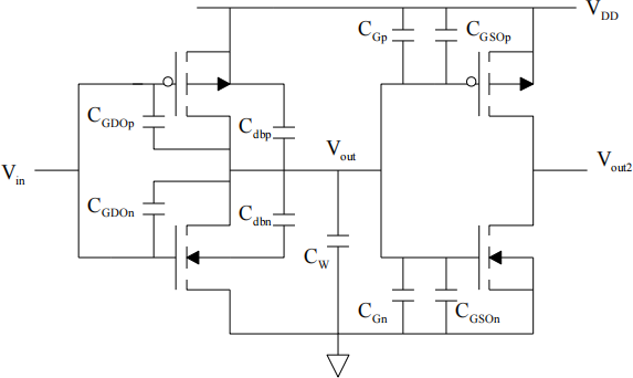
Fig. 1: Unity fan-out CMOS inverter.
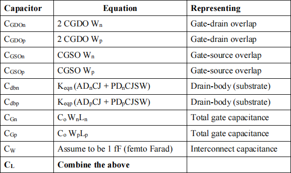
Table 1: Different internal/external capacitances of a CMOS inverter.
CGDO, CGSO, ADn, ADp, CJ, CJSW are SPICE parameters obtained from a SPICE netlist with values given in Table 2. Parameters, W and L are the channel width and channel length, and Co is the gate (oxide) capacitance per unit area. The overlap capacitances, CGDO and CGSO can be represented as,
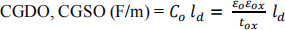
where εo = 8.85 × 10- 12 F/m, εox = 3.9 and ld is the lateral diffusion.
The drain-body (or substrate) capacitances (Cdbn, Cdbp) are related to the capacitance of the depletion region associated with the drain/substrate junction for the n-channel MOST and p-channel MOST respectively. These capacitances are dependent on the area (AD) and perimeter (PD) of the regions, and a factor, Keq that takes into account the voltage dependence of Cdb. The junction depletion capacitance can be given as:
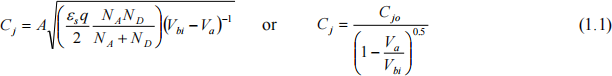
where NA, ND are the average doping levels of the drain contact and substrate or body regions, Va is the voltage across the junction and Vbi is the built-in voltage of the junction given as,
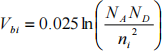
where ni is the intrinsic carrier concentration = 1.5 x 10¹⁶ m-3. For the p-channel MOSFET , you will need to estimate the n-well doping (in which the p-channel device sits). You can assume the doping of then-well to be a factor of 10 higher than the substrate doping. The non-linear capacitance in Eqn. 1.1 can be conveniently written as a linear capacitance Ceq such that for a given voltage swing, the same amount of charge is switched and thus,
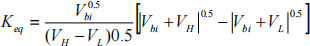
Here VH and VL represent the voltage swing of interest and Ceq = KeqCjo. (Note that to compare with the theory developed in the lectures, you would need to take 90% and 10% levels).
Note that there area number of approximations made when estimating the load capacitance using this approach. Ofcourse, the SPICE simulation uses much more accurate models for the capacitances. You should consider this when comparing theoretical and simulated values of the fall-time. Refer to textbooks for further information.
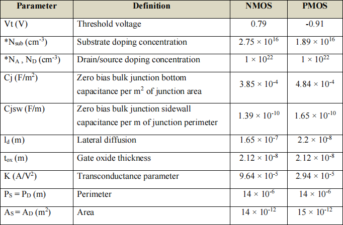
Table 2: SPICE parameters for 1.2 “m CMOS technology (MOS - level 3 on Multisim)for use in the calculations. (*need to convert into SI units!)
Appendix B: Helpful hints
1. Use your notes from ELEC372/472 to help you understand what you are doing.
2. Quote all numerical values in SI units using appropriate prefixes:
10-3 = milli = m
10-6 = micro = μ
10-9 = nano = n
10- 12 = pico = p
10- 15 = femto = f
e.g.: BAD - A capacitance quoted as '2.3456256E- 13'
WHY? - (1) no units, (2) not in SI and (3) too many decimal places
This conveys to the reader that you have pressed buttons on a calculator and have no feel for what you are doing. What do you expect the capacitance values to be; nF? pF? (check in a book if you are not sure - or ask.)
GOOD: quote either as 0.2 pF or better, 235 fF.
ALWAYS THINK ABOUT THE VALUES YOU GET - ARE THEY REASONABLE?
3. Note that some SPICE capacitances have units of 'farads per unit width', i.e. F/m.