关键词 > CSSE2010/7201
CSSE2010/7201 - Introduction to Computer Systems
发布时间:2021-08-27
Hello, dear friend, you can consult us at any time if you have any questions, add WeChat: daixieit
CSSE2010/7201 - Introduction to Computer Systems
Assignment 1 - Digital Logic Design
Semester 2, 2021
Part 1
Part 1 is a timed (1-hour) Blackboard quiz (similar to the weekly quiz format) which you need to complete in a single at-tempt within 1 hour. The quiz will be available from Wednesday 1 Sep 8:00AM AEST and must be completed by Friday 3 September 4:00pm AEST (i.e. the quiz must be started by 3:00PM AEST to have 1 hour to complete it). The quiz will be auto-submitted once 1 hour has passed.
Late penalties as per the ECP apply for any completion after the due date and time, unless you have an extension approved.
This quiz will be of similar format and complexity as the mid-semester exam in the past years and you can use the past mid-semester exams (made available on Blackboard) to practice.
Part 2
Part 2 is to design and simulate a digital circuit for the problem specification given below. This will consist of three tasks:
● Design Task: Design a circuit for the problem description given below.
● Simulation Task: Simulate the circuit you designed in Logisim (or Logisim Evolution).
● Questions: Provide written answers to a few questions about your design.
You are required to submit a single zip file containing the steps of your design task and answers to question in PDF format (either handwritten or typeset) and a Logisim (or Logisim Evolution) file. The submission deadline for part 2 is Monday 6 September 4:00PM AEST.
Problem Description
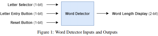
Your task is to design a digital logic system that detects English words at the end of a sequence of letters. These letters will be entered into the system serially (one at a time). The letters in this sequence will be the letters ‘a’ and ‘d’. Two LEDs should be used to display the length (in binary) of the longest word at the end of the sequence entered.
An example of how this circuit should behave is shown in table 1 below.
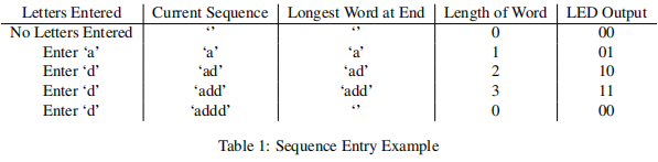
The English words that can be constructed with these two letters are ‘a’, ‘ad’, ‘add’ and ‘dad’.
For this assignment, you will be simulating this detection circuit using Logisim (or Logisim Evolution). The following inputs and outputs will be used to describe the system: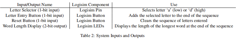
The following rules apply for the system:
● The system starts with an empty sequence of letters, ‘’.
● Letters are added to the sequence by selecting a letter using the Letter Selector and providing a rising edge using the Letter Entry Button.
● The length of the longest word at the end of the sequence is displayed using the two Word Length Display LEDs. These must be labelled L1 (the MSB) and L0 (the LSB).
● When the Letter Selector is 0, the letter ‘a’ is selected. When the Letter Selector is 1, the letter ‘d’ is selected.
● When the Letter Entry Button is pressed (i.e transitions from 0 to 1 thus providing a rising clock edge), the letter selected using the Letter Selector is appended to the sequence. For example, if the current sequence is ‘adda’ and the Letter Selector is 1, when a rising edge is supplied on the Letter Entry button, the sequence becomes ‘addad’.
● If the Reset Button is pressed at any time, the sequence resets to the empty sequence ‘’. This is an asynchronous reset, occurring immediately when the Reset Button is pressed, separate to the main clock provided by the Letter Entry Button. The sequence detector should not operate while the reset button is held down.
Design Task
Your task is to design a digital logic circuit to implement the word detector described above. You should explicitly state any assumptions you make outside the above specifications. As part of the design task you will need to complete the design steps:
1. Draw a state diagram for the word detector described above (hint: you should not require more than 3 flip-flops to build this circuit with a basic encoding). Your state diagram should be complete and drawn according to the standard guidelines mentioned in the lectures and labs. You may not need to include the asynchronous reset input in the state diagram.
2. Create a two-dimensional state table for your state diagram.
3. Choose two possible encodings for the states you have chosen (i.e. binary, gray code or one-hot encoding).
4. Create two state tables (either 1D or 2D) corresponding to each of your two chosen encodings. Note that the 1D state table will have more rows (essentially a truth table) and the 2D state table will be more compact. You can determine the logic expressions (in the next step) from either 1D or 2D state tables.
5. Write boolean expressions for the next state logic and output logic for both chosen encodings. Simplifying these expressions is not required but will make the next steps easier.
6. Choose one encoding scheme to continue with. You might want to analyse the complexity (i.e. how many flip flops, how many gates/chips etc) of your circuit under each encoding scheme before you make this decision. You should not need more than 3 flip flops in total. You will be asked in the questions section to include a justification of why you chose this encoding to continue with.
7. Draw a logic diagram for the word detector circuit given the chosen encoding. You may use gates with more than 2 inputs if needed.
You will need to include all these design steps in the PDF component of your submission.
Simulation Task
As part of the design task you should have drawn a logic diagram for the word detector circuit. The simulation task is to construct this circuit using Logisim (or Logisim Evolution). This Logisim (or Logisim Evolution) file should be submitted in your zip file. Please specify in your PDF submission whether you are using Logisim or Logisim Evolution.
Questions
As part of your submission you should include written answers to the following three questions:
1. In step 6 of the design task, you chose one of two encodings to use for the circuit constructed in Logisim, why did you choose that encoding?
2. If you were to build this circuit using the 74 series chips in the CSSE2010/7201 kit (also visible on the Device Symbols PDF on Blackboard), how many 74 series chips would you need to use? Include some justification of how you calculated this number.
3. How did you test your Logisim circuit to ensure it is working correctly? You may include screenshots if it helps your explanation but they are not necessary.
Submission Process
Your submission should include a zipped folder containing 2 files, a PDF and a Logisim (.circ) file:
● Working for each of the 7 design steps and answers to each of the 3 questions should be included in a PDF file called sXXXXXXX-a1.pdf where sXXXXXXX is replaced by your student number. This may be handwritten or typeset, if it is handwritten, please ensure it is neat and legible.
This zip file should be submitted electronically using Blackboard according to the exact instructions on the Blackboard web-site.● Your Logisim (or Logisim Evolution) file should be included as a .circ file called sXXXXXXX-logisim.circ if you used Logisim or sXXXXXXX-evolution.circ if you used Logisim Evolution. No other simulation tools will be accepted.
You can submit your assignment multiple times before the assignment deadline but only the last submission will be marked. Only submit the zip file described above. You are responsible for ensuring that you have submitted the files that you intended to submit, you are encouraged to download your submission from Blackboard and ensure it contains the correct files. Late penalties will be applied as per the ECP if you submit after the deadline.
Submitted work should be neat, legible and simple to understand - you may be penalised for work that is untidy or diffi-cult to read.
While you can collaborate to clarify any doubts in the learning material required for the assignment, the work you submit must be your own and this is an individual assignment. If any signs of plagiarism/collusion is detected you can be called for an oral assessment as decided by the course coordinator.
Marking Criteria
Part 2 assessment will be marked out of 20 and will be worth 10% of your final grade.
State Diagram - 4 marks
4: Fully correct state diagram.
3: Mostly correct state diagram, with one error.
2: Somewhat correct state diagram, with more than one error.
1: Mostly incorrect state diagram, with many errors.
0: Incorrect state diagram.
State Tables - 2 marks
Marked relative to the given state diagram.
2: Fully correct state tables
1: Mostly correct state tables, with only a few mistakes. Or only one state table for one encoding.
0: No state tables or incorrect state tables.
Boolean Expressions - 3 marks
Marked relative to the given state tables.
3: Correct boolean expressions for all next state and output logic.
2: Mostly correct expressions with only a few minor errors.
1: Somewhat correct expressions with lots of minor errors or a major error/omission.
0: Work with little academic merit.
Logic Diagram - 3 marks
Marked relative to the chosen boolean expressions.
3: Fully correct logic diagram.
2: Mostly correct logic diagram, with a few errors or omissions.
1: Somewhat correct logic diagram, with a lot of errors or omissions.
0: Missing logic diagram or a diagram containing major errors
Logisim Simulation - 5 marks
Circuit functionality marked relative to state diagram.
5: Fully correct Logisim build, uses all specified components and functions correctly according to the problem description.
4: Logisim build that is either fully correct for given state diagram or functions correctly with a minor error.
3: Logisim build that contains a few minor errors resulting in it not achieving the specified circuit functionality.
2: Logisim build with many errors that does not achieve the specified circuit functionality.
1: Logisim build that does not reflect the problem description.
0: Work with little academic merit.
Questions - 3 marks
3: Reasonable answers to all three questions that demonstrate an understanding of the design task.
2: Reasonable answers to two questions that demonstrate an understanding of the design task.
1: Reasonable answer to one question that demonstrates an understanding of the design task.
0: Answers to questions do not reflect an understanding of the design task.