520.424 FPGA Lab 2025 Inference of Latches and Flip-Flops
Hello, dear friend, you can consult us at any time if you have any questions, add WeChat: daixieit
520.424 FPGA Lab 2025
Inference of Latches and Flip-Flops
Before you start, carefully read this project assignment in its entirety and the referenced sections in the textbook. They contain a good deal of information. At the end of this project assignment, there are hand-in questions related to the project. You should look at them before starting the project, and try to answer them as you go.
Textbook sections
For this lab project, review the following sections in the textbook.
• std logic: section 3.5.2.
• Signal assignment: section 4.2.
• Process blocks: sections 5.1 and 5.2.
• Components: section 2.2.2.
Project overview
The objectives of this lab project are to:
1. Gain experience with the Xilinx Vivado software - Create an FPGA project and use the project manager.
2. Start using VHDL - create some VHDL entities with different circuit description modes.
3. Introduce synthesis, and the principles underlying hardware inference.
This simple lab assignment is the vehicle for learning how to go through the end-to-end process of defining, synthesizing, and implementing an FPGA circuit with multiple components. A product of this lab is a D Flip-Flop component with asynchronous reset. This component is a basic digital building block.
This project counts for 100 points, based on your answers to the set of questions at the end of this assignment. As you work through the successive parts of this assignment, you will be able to answer the corresponding questions. You may want to review the questions first.
Answering these questions helps ensure that you understand the technology underlying the assignment. As with all assignments, only the answers to the questions are to be handed in. For instance, do not include screenshots or source code unless a question specifically asks for it.
Please remember that the hand-in answers are to be individual work. Do not ask for any help or hints on the questions.
Overview: The FPGA register element
In digital systems, a D-latch is normally a level-sensitive memory circuit with 3 port signals: an input D, an output Q, and a control (or clock) input C. In a latch, the output Q follows the input D when the control input C is active (either high or low, depending on the design). When the control input C is not active, the output Q holds its last value.
In contrast, a D-flip-flop is normally an edge-triggered memory circuit. It has the same inputs and outputs as a D-latch, but the output Q is updated on a control input edge (either a low-to-high transition or a high-to-low transition, depending on the design). When the control input C is not changing or is of the incorrect edge, the output Q holds its last value.
In Xilinx FPGAs, D-latches and D-flip-flops are implemented by a register element primitive. In this context, a register element is a 1-bit memory device. (Note that in most literature, things called registers are made up of N register elements.) The circuit is called a primitive because it is a monolithic circuit which is not synthesized by combining other logic circuits. Most Xilinx primitives can be configured to act like different digital logic gates. So, for instance, D-latches with active high or low control inputs and D-flip-flops with rising-edge or falling-edge control inputs, regardless of whether or not they have any asynchronous set/reset inputs, are all implemented by the same Xilinx register element primitive.
Note that Xilinx FPGAs also contain primitives for implementing combinatorial logic such as AND and OR gates. These primitives could be used to create memory circuits, but one of the main purposes of this lab project is to demonstrate why this is not a wise thing to do.
Additionally, Xilinx FPGAs also contain dedicated low-skew signal networks for carrying clock signals to flip-flops and latches. However, there are only a limited number of these networks, and the other purpose of this lab is to demonstrate why not using these features is also a unwise.
Part A - Structural versus behavioral description
In the first part of the lab project, you will enter the VHDL code to describe a simple set-reset latch in two different ways: a structural description and a behavioral description. For the structural description, we will use VHDL to describe the following digital circuit:
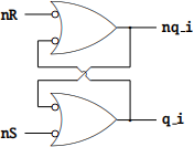
Note that this set-reset latch is active low – that is, the idle state is when set (nS) and reset (nR) are both 1. In the idle state, q i and nq i are complementary and retain their state. If nS is 0 and nR is 1, q i goes to 1 and nq i goes to 0. Conversely, if nS is 1 and nR is 0, q i goes to 0 and nq i goes to 1. We can describe this circuit with the following VHDL code:
library IEEE;
use IEEE .std_logic_ 1164 .all;
entity SRLATCH1 is
port(
nS: in std_logic;
nR: in std_logic;
Q: out std_logic
);
end SRLATCH1;
architecture arch of SRLATCH1 is
signal q_i: std_logic;
signal nq_i: std_logic;
begin
Q<=q_i;
q_i<=(not nq_i) or (not nS);
nq_i<=(not q_i) or (not nR);
end arch;
The core of the VHDL description is in the last two lines before the end arch; statement. The rest of the code is for declarations: to include libraries, to describe the inputs and outputs of the circuit, and to declare internal signals. Note that in this example, the output Q of the circuit is distinct from the OR gate’s output. This is done to overcome a VHDL limitation that disallows output ports from appearing on the right-hand side of an assignment.
The alternative behavioral description uses VHDL to describe the desired behavior of the circuit. This is done using an if statement within a process:
library IEEE;
use IEEE .std_logic_ 1164 .all;
entity SRLATCH2 is
port(
nS: in std_logic;
nR: in std_logic;
Q: out std_logic
);
end SRLATCH2;
architecture arch of SRLATCH2 is
begin
process(nS,nR)
begin
if (nS=’1’) and (nR=’0’)
then
Q<=’0’;
elsif (nS=’0’) and (nR=’1’)
then
Q<=’1’;
end if;
end process;
end arch;
In this case, we only specify what we want to happen when the set or the reset input becomes active (with the other inactive). The Vivado software understands that Q should retain its state if none of the if conditions in a process are satisfied.
Project creation and code entry
Review the tutorial on the course web site for detailed instructions on creating and simulating your project. Although the exact FPGA type is not critical for this lab assignment, you should get into the habit of specifying the correct type (typically by selecting the Digilent Cmod A7 board).
Simulation
The next step is to perform a functional simulation of the VHDL descriptions. A sample test bench for SRLATCH1 is shown below:
library IEEE;
use IEEE .std_logic_ 1164 .all;
entity SRLATCH1_TB is
end SRLATCH1_TB;
architecture arch of SRLATCH1_TB is
component SRLATCH1
port(
nS: in std_logic;
nR: in std_logic;
Q: out std_logic
);
end component;
signal nS: std_logic:=’1’;
signal nR: std_logic:=’1’;
signal Q: std_logic;
begin
test: SRLATCH1 port map (nS=>nS,nR=>nR,Q=>Q);
process
begin
nS<=’1’;nR<=’1’;
wait for 1 us;
nS<=’0’;nR<=’1’;
wait for 1 us;
nS<=’1’;nR<=’1’;
wait;
end process;
end arch;
Note that this only simulates a single nS pulse. You will need to add many more steps to fully simulate SRLATCH1 and SRLATCH2. Indeed, because these circuits have memory, it is not sufficient to apply all four input combinations. For this particular circuit, you must simulate all possible input transitions:
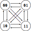
With two inputs, there are twelve possible transitions. However, it is not easy to fully traverse the above graph without repeating some transitions, so the actual number of transitions you use may be somewhat larger.
You should recall from your background in digital logic that the set-reset latch implementation using cross-coupled logic gates as in SRLATCH1 has a troublesome behavior when both nS and nR are active. Your simulation will possibly fail when you transition in to or out of that state. So when you have identified the problem transition, move it to the end of the simulation test bench so that all the other (working) transitions occur first.
Use the same sequence to test SRLATCH2 and verify that it does not exhibit any troublesome transitions.
Simulator limitations
The actual hardware may behave differently from the simulation, because the simulator doesn’t perfectly model the behavior of the electronic circuit. The trade-off is that more detailed modeling of the circuit behavior requires more computations and therefore will result in a slower simulation. The simulator in Vivado is therefore designed for a good balance between fidelity and performance.
In particular, when performing a functional simulation of a VHDL module, the simulator does not incorporate dynamic effects such as propagation delay. (Simulations with dynamic effects can be performed post-synthesis or post-implementation.) However, we can emulate the effects of propagation delay to see if it alters the simulation results for SRLATCH1 and SRLATCH2. To do this, modify the body of SRLATCH1 as follows:
Q<=q_i;
q_i<=(not nq_i) or (not nS) after 0 . 1 us;
nq_i<=(not q_i) or (not nR) after 0 . 1 us;
Similarly, modify the body of SRLATCH2 as follows:
process(nS,nR)
begin
if (nS=’1’) and (nR=’0’)
then
Q<=’0’ after 0 . 1 us;
elsif (nS=’0’) and (nR=’1’)
then
Q<=’1’ after 0 . 1 us;
end if;
end process;
Re-run your simulations and check if the behavior is different. Note that the propagation delay used here is much larger than the actual propagation delay of the FPGA, but is chosen to make the effect easier to see in the simulation. Also note that the wait for and after statements are only useful in simulations, as they are ignored by the synthesizer. Therefore these statements should really only be used in test benches.
Part B - Toggle Flip-Flop Counter
In the second part of the lab project, you will write your own VHDL code for a rising-edge D-flip- flop with an asynchronous reset input. This element will then be used to create a cascade counter or toggle flip-flop counter to see why it is unwise to use such a circuit. (In part C we will see how to properly construct a binary counter.) The reset input must be active high, and the reset state should be D=0. You must call this entity DFFAR (D Flip-Flop with Asynchronous Reset) and use the following entity declaration:
entity DFFAR is
port(
D: in std_logic; -- Data input
C: in std_logic; -- Clock input
R: in std_logic; -- Asynchronouse reset
Q: out std_logic -- Data output
);
end DFFAR;
Note that we want asynchronous behavior for the reset input. This means that the effect of the control signal is independent of when it is asserted relative to the clock’s edge. In expressing this behavior, it helps to remember that any if statement expresses prioritized conditions in the circuit behavior.
In your code, use an explicit rising edge test, rather than a wait until rising edge as the latter may not synthesize. Also, do not get in the habit of combining tests of other signals with the if rising edge test of a clock. This also may not synthesize, and it does not lend itself to the “two-segment” approach to clock driven processes (which we will cover later in the semester).
Create the DFFAR.vhd file and add it to your project. Then you should run a functional simulation to check its operation. For this, you can re-work the SRLATCH1 TB test bench to test your DFFAR implementation. Make sure your simulation tests all the requisite behaviors.
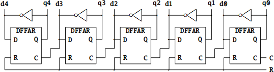
Cascade Counter
Create another module called tcounter that takes an input clock C, an asynchronous reset control input R and outputs a 5-bit vector bits. The entity declaration should be:
entity tcounter is
port(
C: in std_logic; -- Clock input
R: in std_logic; -- Asynchronouse reset
B4: out std_logic; -- Output bits
B3: out std_logic;
B2: out std_logic;
B1: out std_logic;
B0: out std_logic
);
end tcounter;
The DFFAR entity must be instantiated as a component in the counter. Use the following circuit diagram to guide your VHDL construction.![]()
Don’t forget that you will need to declare the DFFAR entity as a component in the VHDL for the counter. The component declaration should be:
component DFFAR
port(
D: in std_logic; -- Data input
C: in std_logic; -- Clock input
R: in std_logic; -- Asynchronouse reset
Q: out std_logic -- Data output
);
end component;
The instantiation for each DFFAR should look something like:
dffar2: DFFAR port map (
D=>d2,
C=>d1,
R=>R,
Q=>q2
);
You will also need to infer the inverters by creating assignments for d0 through d4:
d4=>not q4;
d3=>not q3;
d2=>not q2;
d1=>not q1;
d0=>not q0;
Be sure to correctly assign the C input for each instance. Note that as for SRLATCH1, the counter module tcounter outputs B0 through B4 cannot be used as an input. Therefore, you cannot use D=>not B2 and must instead use an intermediate signal (q2 in this example). You must also include assignments such as B2<=q2; somewhere in your architecture body. Be sure to do this for all five outputs.
As before, add the module tcounter.vhd to your project and run a functional simulation to check its operation. You will need to create a test bench that generates the clock and asynchronous reset signals. An example of how to do this is shown below:
process
begin
C<=’0’;
wait for 1 us;
C<=’1’;
wait for 1 us;
end process;
process
begin
R<=’1’;
wait for 2 . 5 us;
R<=’0’;
wait;
end process;
Note how the process for the reset signal R has a wait statement at the end. This prevents the process from automatically repeating, as it does in the case of the clock signal C.
The functional simulation will show all the bits changing instantaneously on every clock edge. As this is not realistic, add a delay in the DFFAR module. For instance, where you have:
Q <= D;
change it to:
Q <= D after 0 . 1 us;
Make sure that your delay value is not too long: you want the counter to settle before the next clock edge.
Part C - Binary Counter
To build a proper counter, we need an additional circuit element: a half-adder. Use the following module for your half-adder:
library IEEE;
use IEEE .std_logic_ 1164 .all;
entity HADD is
port(
X: in std_logic; -- Data in
Y: in std_logic; -- Data in
C: out std_logic; -- Carry out
S: out std_logic -- Sum out
);
end HADD;
architecture arch of HADD is begin
C<=X and Y;
S<=X xor Y;
end arch;
Then assemble your counter by instantiating HADD and DFFAR modules as needed, using the following circuit diagram as a guide. Note that you will need to declare local signals c0 to c3 in addition to d0 through d4 and q0 through q4.
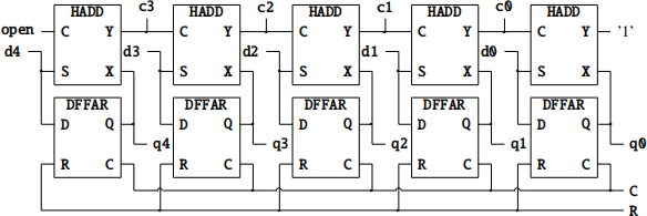
Your counter entity declaration and component declarations should look like:
library IEEE;
use IEEE .std_logic_ 1164 .all;
entity bcounter is
port(
C: in std_logic; -- Clock input
R: in std_logic; -- Asynchronouse reset
B4: out std_logic; -- Output bits
B3: out std_logic;
B2: out std_logic;
B1: out std_logic;
B0: out std_logic
);
end bcounter;
architecture arch of bcounter is
component DFFAR
port(
D: in std_logic; -- Data input
C: in std_logic; -- Clock input
R: in std_logic; -- Asynchronouse reset
Q: out std_logic -- Data output
);
end component;
component HADD
port(
X: in std_logic;
Y: in std_logic;
C: out std_logic;
S: out std_logic
);
end component;
signal d4: std_logic;
signal d3: std_logic;
signal d2: std_logic;
signal d1: std_logic;
signal d0: std_logic;
signal q4: std_logic;
signal q3: std_logic;
signal q2: std_logic;
signal q1: std_logic;
signal q0: std_logic;
signal c3: std_logic;
signal c2: std_logic;
signal c1: std_logic;
signal c0: std_logic;
begin
B4<=q4;
B3<=q3;
B2<=q2;
B1<=q1;
B0<=q0;
...
end arch;
Note that the first half-adder has a constant input on Y and the last half-adder has an unconnected output on C. As shown in the diagram, in the instantiation of the first half-adder you will use:
Y=>’1’,
and in the instantiation of the last half-adder you will use:
C=>open,
The open keyword is used in VHDL when the output of a module is not needed – it cannot be used on inputs.
You can use the same test bench to test this counter by replacing the instantiation of tcounter with bcounter. You should be able to confirm that even with the assignment delay in DFFAR, the counter outputs are still aligned. (You can add delays to the half-adders as well.)
Grading
The overall project will count 100 points:
100 pts - Answers to questions:
1. (8 pts) For SRLATCH1 and SRLATCH2, we simulated twelve different input transitions. Explain why performing a functional simulation for all twelve possible input transitions for an arbitrary digital circuit that has only two inputs may be insufficient to exhaustively cover all the functional behavior of the circuit. (Note that in a functional simulation, we intentionally ignore the dynamic or temporal effects, so these are not acceptable answers to this question.)
2. (8 pts) During functional simulation of SRLATCH1, what input transition (e.g. 10 → 01) causes the simulation to terminate with a fatal error? What is the error message?
3. (8 pts) During functional simulation of SRLATCH1 with the delayed output, you should no longer get a fatal error at the previously problematic input transition. What does the simulation show instead?
4. (4 pts) What behavior would a real physical implementation of SRLATCH1 exhibit for the input transition that was problematic in the simulation?
5. (8 pts) In the test bench SRLATCH1 TB, what error message do you get if you specify wait for 1000 ns; instead of wait for 1 us;, and why?
6. (8 pts) In SRLATCH1, what error message do you get if you replace q i with Q in the body of the module as shown on the next page and attempt to simulate? Why?
architecture arch of SRLATCH1 is
signal nq_i: std_logic;
begin
Q<=(not nq_i) or (not nS);
nq_i<=(not Q) or (not nR);
end arch;
7. (8 pts) What trivial changes would you make to the tcounter entity to make it count down instead of up, with the R control input forcing the output B to all ones. (Note: you are not permitted to modify the DFFAR module.)
8. (8 pts) What trivial changes would you make to the tcounter entity to make it count down instead of up, with the R control input forcing the output B to all zeros. (Note: you are not permitted to modify the DFFAR module.)
9. (8 pts) When simulating tcounter, the simulator initially shows all the signals being updated instantaneously. After adding the propagation delay to the DFFAR module, do the B4 through B0 signals update simultaneously or in a staggered fashion?
10. (8 pts) How many clock signals are present in tcounter in part B? (A clock signal is any signal used with a rising or falling edge test.)
11. (4 pts) What erroneous behavior does tcounter exhibit if the propagation delay is increased from 0. 1μs to 0.5μs?
12. (8 pts) When simulating bcounter, and after adding the propagation delay to the DFFAR module, do the B4 through B0 signals update simultaneously or in a staggered fashion?
13. (8 pts) How many clock signals are present in bcounter in part C?
14. (4 pts) Consider the following broken behavioral construct for inferring a DFF with an active high reset.
if rising_edge(clk)
then
Q<=D;
elsif (reset=’1’)
then
Q<=’0’;
end if;
According to this circuit description, if reset and D are both high, what do you think should happen to Q on the rising edge of clk?
2025-09-19