EECT/CE 6325 VLSI DESIGN Final Project
Hello, dear friend, you can consult us at any time if you have any questions, add WeChat: daixieit
EECT/CE 6325 VLSI DESIGN
Final Project
4-bit Microprocessor
Assignment
You and your partner will design, layout, and simulate a 4-bit calculator that performs the following functions:
1) Addition of two 4-bit positive numbers
2) Subtraction of two 4-bit positive numbers
3) Multiplication of a 4-bit positive number by 2, 4, and 8
4) Division of a 4-bit positive number by 2, 4, and 8
This design follows the structure of a finite state machine -- the output of each computation will be used as an input to the next step. The clock is provided externally. The clock signal is a series of voltage pulses, swinging from GND = 0 V to VDD = 1.2 V with a 50% duty cycle and 50 ps rise and fall times. The load capacitance connected to the outputs of the calculator is to be 50 fF.
Milestones
Due April 2: Draw a complete block diagram that performs these tasks. (10 points)
Due April 9: Learn to use hierarchical design in schematics and layout. Learn to create a series of signals in HSpice. Draw a floorplan of your calculator. The floorplan includes the estimated geometric positioning of the layouts of different elements that considers continuous power rails ( VDD and GND) across different cells and cascading. Submit the floorplan. (10 points)
Due April 16: Design and simulate your transistor-level calculator schematic in Cadence. (20 points)
Due April 30: Finish the layout of your design. Show that a large portion of your schematic passes DRC/LVS. (10 points)
Due May 7: Complete project with simulation of extracted layout. Prepare for a 5- minute class presentation demonstrating functionality, showing metrics, and explaining design choices. (30 points for completion, 20 point design competition)
Grading
You and your partner will receive the same grade. The final assignment will partially be graded comparatively, with the highest grade going to the group with the lowest area- energy-delay product, AEDP, defined as the area of the minimum bounding rectangle that encloses the full layout multiplied by the minimum possible clock period and the energy consumed to perform a set of testbench operations to be declared on April 30. You must declare what the clock frequency should be for the testing to verify functionality. Each operation is triggered by a positive edge of the clock and finished within one clock cycle. No late assignments will be accepted for any milestone.
Appendix
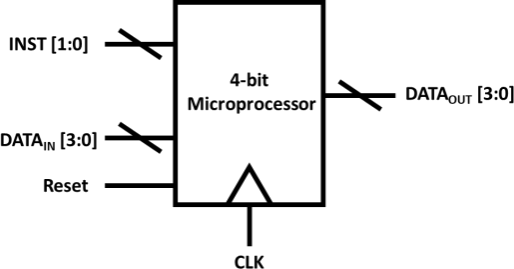
Instruction Set Architecture
INST [1:0] = 00: Addition; DATAOUT [3:0] (n) = DATAOUT [3:0] (n-1) + DATAIN [3:0] (n)*
INST [1:0] = 01: Subtraction; DATAOUT [3:0] (n) = DATAOUT [3:0] (n-1) – DATAIN [3:0] (n)*
INST [1:0] = 10: Multiplication; DATAIN [2:0] (n) = 100, 010, 001 means multiplication by 8, 4, 2 on DATAOUT [3:0] (n-1)*,#
INST [1:0] = 11: Division; DATAIN [2:0] (n) = 100, 010, 001 means division by 8, 4, 2 on DATAOUT [3:0] (n-1)*,#
*Neglect the overflow bits
# Multiplication/Division by 000, 011, 101, 110, and 111 is not required
Sample Set of Operations
Reset: DATAOUT = 0000 [Done with the reset input]
Operation 1 INST[1:0] = 00, DATAIN = 0101 DATAOUT = 0101
Operation 2 INST[1:0] = 01, DATAIN = 0011 DATAOUT = 0010
Operation 3 INST[1:0] = 00, DATAIN = 0001 DATAOUT = 0011
Operation 4 INST[1:0] = 10, DATAIN = 0111 DATAOUT = 0011
Operation 5 INST[1:0] = 10, DATAIN = 1011 DATAOUT = 0011
Operation 6 INST[1:0] = 11, DATAIN = 0011 DATAOUT = 0011
Operation 7 INST[1:0] = 10, DATAIN = 0010 DATAOUT = 1100
Operation 8 INST[1:0] = 11, DATAIN = 0001 DATAOUT = 0110
Testing and Verification
DATAIN [3:0] and type/order of operations should be flexible in the design. A list of operations and operands (like the sample one) and the testbench generator script will be posted on April 7.
2025-05-22
4-bit Microprocessor