ECSE 433 – Physical Basis of Semiconductor Devices
Hello, dear friend, you can consult us at any time if you have any questions, add WeChat: daixieit
ECSE 433 – Physical Basis of Semiconductor Devices
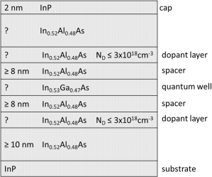
6. Design a quantum-well heterostructure for a high-electron mobility transistor (HEMT) that is lattice matched to an InP substrate operating at 300 K. The materials that you have available are InP, In0.53Ga0.47As and In0.52Al0.48As, arranged as in the example below.
In developing your design, you may choose from one of three design strategies:
two doping layers, one above and one below the quantum well, as shown above
a single doping layer above the quantum well
a single doping layer below the quantum well
Several design criteria must be satisfied:
a. to ensure surface stability, the surface must be terminated with a 2 nm thick InP cap [+1pt]
b. to avoid low-mobility conduction, the first (lowest energy) sub-band must be confined to a single undoped quantum well [+1pt]
c. the maximum doping density permitted in any layer is ND = 3x1018cm-3 [+1pt]
d. to minimize mobility reduction by ionized impurity scattering, the spacer layer thickness between the quantum well heterointerfaces and any doping layer must be at minimum 8 nm [+1pt]
e. the total electron sheet density must exceed ntot = 1.8x1012 cm-2 [+3pts]
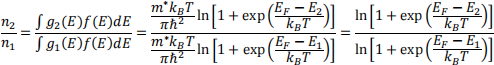
f. to minimize inter-sub-band scattering and mobility loss, the ratio of electron density in the second sub-band to the first sub-band must satisfy n2/n1 ≤ 0.01 [+3pts]
You will find it useful to consider carefully:
the relative merits in choosing the number and location of doping layers
the expected effects of varying the different layer thicknesses upon the accessible electronic states and the population of those electronic states with electrons
Since design is competitive, bonus points will be awarded for the design that meets all the design criteria listed above, and that achieves the following:
the highest electron sheet density [+3 bonus points]
the minimum distance between quantum well heterointerface and the semiconductor surface [+3 bonus points]
In the event of tied performance amongst several designs, bonus points will be divided equally amongst authors of the winning designs.
Software: Use the open access MATLAB package Q_SchrodingerPoisson1D_CB*, distributed together with this assignment with several minor modifications implemented for ease of use. This package was written by L. Nevou at TUWien, implementing self-consistent solution of the Poisson (Gauss) and Schrodinger equations for conduction band electrons in semiconductor heterostructures.
The heterostructure design for simulation is specified in input_file.m .
The simulation is executed with SchrodingerPoisson1D_CB_Kane_Main.m .
Two figures will be produced with the simulation results, as well as printed output of the sub-band energies and Fermi energy.
*original source: Laurent NEVOU (2025). Q_SchrodingerPoisson1D_CB
(https://github.com/LaurentNevou/Q_SchrodingerPoisson1D_CB), GitHub.
Retrieved 7 III 2025.
Your design submission must include the following seven items:
1. A complete structure description, wherein each layer is specified with semiconductor type (InP, AlInAs or InGaAs), a thickness (in nm), and doping density (in 1018 cm-3). This can be extracted from input_file.m.
2. A plot of the energies (conduction bands, sub-band energies, Fermi energy), charge carrier density, and wavefunction amplitude versus depth z. This is figure 1 produced by the program.
3. The depth of the quantum well top heterointerface d in units of nm from the semiconductor surface.
4. The total electron sheet density ntot in units of cm-2. This is indicated in figure 1.
5. The four lowest sub-band energies (E1 to E4), and the Fermi energy EF. This is provided by the program output.
6. A quantitative calculation of the fraction, n2/n1, of the density of electrons residing in the second sub-band relative to the first sub-band. This can be approximated from the ratio:
7. A brief statement (several sentences will suffice) on the strategy that you used to meet the design criteria specified on page 6.
2025-04-17