ELEE08016 ANALOGUE CIRCUITS 2
Hello, dear friend, you can consult us at any time if you have any questions, add WeChat: daixieit
ANALOGUE CIRCUITS 2
ELEE08016
![]() SECTION A
SECTION A
Question A1
1a)
In your own words, describe the purpose of biasing a transistor. Your
description should not normally exceed 250 words. (3)
1b)
Figure A1a shows a transistor amplifier circuit. Explain the reasons this
circuit is not often used in commercial production. (3)
1c)
Describe the features of bipolar transistor performance that are modelled by each component of the Hybrid-π model.
(2)
1d)
Identify the transistor characteristic that is the main source of non- linearity in bipolar transistor based designs.
(2)
2a)
Draw a circuit schematic with a high pass filter at the input of a buffer
amplifier and a low pass filter at the output. (3)
2b)
Sketch the amplitude Bode plot approximations for the circuit in 2a), labelling the location of the cut-off frequencies and the slope of the
amplitude response. (4)
2c) Why is a buffer amplifier used in a circuit? (1)
2d)
An operational amplifier has a unity gain bandwidth of 10 MHz and a dominant cut-off frequency in its open loop response of 100 Hz, What
is the open loop gain (dB) of the operational amplifier? (2)

Figure A1a
![]()
![]()
![]()
![]()
![]()
![]() SECTION B
SECTION B
Question B1
In the following question, where not otherwise specified, make reasonable assumptions for transistor parameters.
Figure B1a shows an amplifier with dual-feedback biasing. You may assume that the input and output capacitors are sufficiently large that they can be ignored for the frequencies of interest.
a) Draw the small-signal model for Figure B1. (3)
b) Show that the gain of the circuit is:
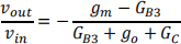
where go = 1/ro, Gc = 1/Rc, and GB3 = 1/RB3. (3)
c) Determine an expression for the amplifier output resistance. (4)
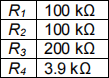
Figure B1d shows an op-amp based amplifier circuit.
d) Determine the gain of the circuit for the following component values:
e) State the input impedance of the amplifier. (1)
f) Discuss the advantage of this design compared to a standard inverting
op-amp design that achieves the same gain. (2)
g) If VSS = − VDD . modify the circuit to use a single-sided power supply of
0 V and VDD . (3)
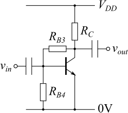
Figure B1a
![]()
![]()
![]()
![]()
![]()
![]()
![]()
![]()
![]()
![]()
![]()
![]()
![]()
![]()
![]()
![]()
![]()
![]()
![]()
![]()
![]()
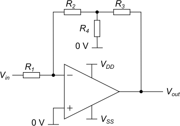
Figure B1d
Question B2
a) For the circuit shown in Figure B2a, show that the voltage gain Av is
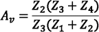
(2)
|
b) |
For Z1 = 1 kΩ, Z2 = 0.1 µF, Z3 = 500 Ω , and Z4 = 1 kΩ, derive an expression for the transfer function of the amplifier circuit. Express the transfer function in a standard form or a product of forms, i.e., constant jω, low pass, inverted low pass or high pass forms. |
|
|
(4) |
c)
Calculate the cut-off frequency (Hz) and gain (dB) of the amplifier circuit.
(4)
d) Write down an expression for the transfer function of the amplitude response shown in the Bode plot of Figure B2d. (4)
|
e) |
Using the circuit topology in Figure B2a, derive relative component values for Z1 to Z4 to produce the Bode plot of Figure B2d, if Z1 and Z4 are capacitors, Z2 and Z3 are resistors. |
|
|
(6) |
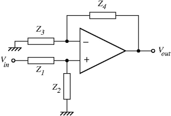
Figure B2a)
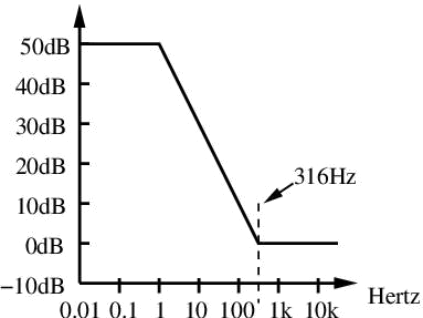
Figure B2d)
2021-12-15