ELEE11044 ANALOGUE IC DESIGN
Hello, dear friend, you can consult us at any time if you have any questions, add WeChat: daixieit
ANALOGUE IC DESIGN
ELEE11044
SECTION A
Question A1
a) Give TWO possible factors that contribute to DC offset in a MOSFET (2) differential amplifier design.
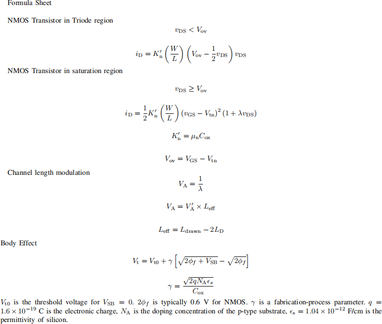
A circuit designer intending to operate a MOSFET in saturation is considering the effect of changing the device dimensions and operating voltages on the drain-
source current, ![]()
![]() . If channel-length modulation is negligible, that is
. If channel-length modulation is negligible, that is ![]() = 0, determine the factor by which
= 0, determine the factor by which ![]()
![]() changes in each of the following cases.
changes in each of the following cases.
b) (i) The channel length is doubled, (1)
(ii) The channel width is doubled, (1)
(iii) The overdrive voltage is doubled, (1)
(iv) The drain-to-source voltage is doubled. (1)
c) Briefly discuss channel-length modulation and show that the drain- (4) source resistance, rDS , of a MOSFET transistor is given as:
Take ![]()
![]() as the drain-source current with channel-length modulation.
as the drain-source current with channel-length modulation.
d) Digital to analogue (DAC) converters may be characterised by their conversion time or scaling method.
(i) Name two basic DAC architecture types based upon
conversion time and state their relative conversion speed. (1)
(ii) Name three different scaling methods used in DACs. (2)
e) With reference to a DAC characteristic define
(i) Integral nonlinearity, (1)
(ii) Differential nonlinearity, (1)
(iii) Monotonicity. (1)
f) How do the following operational amplifier performance characteristics affect DAC performance?
(i) Settling time, (2)
(ii) Slew rate. (2)
SECTION B
Question B1
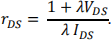
An NMOS amplifier with diode-connected active load is shown in Fig. B1 on the next page. The channel-length modulation effect of this amplifier is not negligible, that is λ ≠ 0.
a) Draw a well-labelled small-signal model of the diode-connected active (5) load amplifier.
b) Use the model in Question B1a) to derive the voltage gain expression (3) for the amplifier of Fig. B1.
c) Briefly discuss TWO limitations of the diode-connected active load (4) NMOS amplifier shown in Fig. B1 on the next page.
A basic current-mirror design is shown in Fig. B1a on the next page, the two transistors M1 and M2 are matched with channel length of 1 µm, channel width of 10 µm, threshold voltage, ![]()
![]() = 0.7 V and
= 0.7 V and ![]()
![]() = 200 μA⁄V2A. The supply voltage,
= 200 μA⁄V2A. The supply voltage, ![]()
![]() = 3 V and
= 3 V and ![]()
![]()
![]() = 100 μA. By neglecting channel-length modulation, determine:
= 100 μA. By neglecting channel-length modulation, determine:
d) the value of resistor, R. (2)
e) The minimum value of the DC output voltage, ![]() 0 , required to keep transistor M2 in saturation. (2)
0 , required to keep transistor M2 in saturation. (2)
For the basic current mirror of Fig. B1a, if the channel-length modulation is no longer negligible and the chip fabrication process has an Early voltage, ![]()
![]() ′ = 20 V⁄μm. Determine:
′ = 20 V⁄μm. Determine:
f) the output resistance, ![]()
![]() 2 , of the current sink. (2)
2 , of the current sink. (2)
g) The change in output current, ![]() 0 , resulting from a +1 V change in
0 , resulting from a +1 V change in ![]() 0 . (2)
0 . (2)
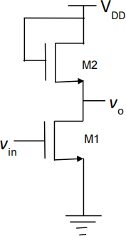
Fig. B1: An NMOS amplifier with
a diode-connected active load.
Question B2
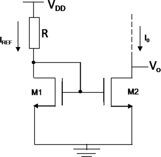
a) Draw the small-signal model for the two-transistor amplifier circuit (4) shown in Fig. B2 on the next page. Find the small-signal gain of the circuit.
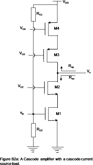
The cascode amplifier with a cascode current source shown in Fig. B2a on the next page is operated at a current of 0.2 mA with all devices at |![]() ov| = 0.2 V. If all the devices also have |
ov| = 0.2 V. If all the devices also have |![]() A | = 2 V, determine:
A | = 2 V, determine:
b) the transconductance, ![]()
![]() 1 , of the NMOS transistor M1. (2)
1 , of the NMOS transistor M1. (2)
c) The voltage gain, ![]() V , realised. (4)
V , realised. (4)
Consider a 2-stage Miller CMOS operational amplifier with 1 MHz gain bandwidth to be used in a voltage follower or buffer configuration.
d) If the dominant pole of the amplifier is 100 Hz, determine the low frequency open loop gain, Av0 , of the operational amplifier in decibels. (2)
e) If a phase margin of 45o is required, determine the frequency of the non- dominant pole. (2)
f) Sketch a Bode plot approximation of the
(i) Loop gain of the operational amplifier, (3)
(3)
(ii) Phase response of the operational amplifier.
Fig. B2: Two Transistor (CMOS) Amplifier
Question B3
Consider the folded cascode operational amplifier in Figure QB3.
The drain current of transistor M11 is 0.1 mA. The drain currents of transistors M9 and M10 are both 0.15 mA. Assume K’N = 100 ![]() A/V2 and K’P = 40
A/V2 and K’P = 40 ![]() A/V2 . Assume for all transistors
A/V2 . Assume for all transistors ![]() = 0.05 V-1 , |
= 0.05 V-1 , |![]()
![]() | = 0.75
| = 0.75 ![]() , the overdrive voltage (VGS – Vt) = 0.2 V and L = 1
, the overdrive voltage (VGS – Vt) = 0.2 V and L = 1 ![]() m.
m.
Assume the power supply voltages are ± 2.5 ![]() and CL = 2 pF.
and CL = 2 pF.
a) Find the W/L ratio of the transistors M1/2, M3/4, M5/6/7/8, M9/10 and
M11, stating any assumptions made. (6)
b) Determine the input common mode voltage range and the output voltage range of this operational amplifier. (4)
c) Determine the DC gain of the amplifier. (6)
d) Determine the dominant pole frequency and the unity gain bandwidth. (2)
e) Determine the slew rate and power consumption of the amplifier. (2)
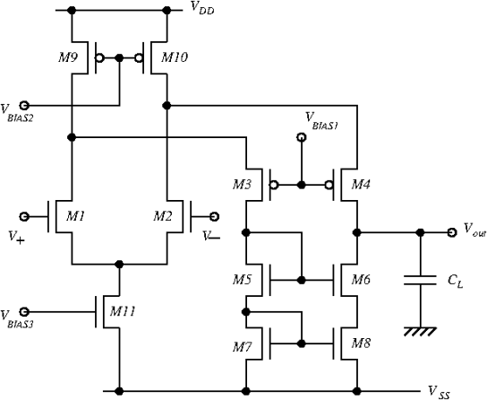
Figure B3
2021-12-15