ELEC372/472: Integrated Circuit Design Assignment 3
Hello, dear friend, you can consult us at any time if you have any questions, add WeChat: daixieit
ELEC372/472: Integrated Circuit Design Assignment 3
Objectives:
. To understand the fundamental concepts underlying the behaviour of an operational amplifier (Op-amp) as covered in ELEC372/472 in the context of design.
. To design asingle-stage Op-amp using a 1.2 µm CMOS technology with specified input and output conditions. This requires initially calculating the aspect ratios of all transistors in the design, followed by simulating the design on MultiSim, and verifying key findings to those in the specification.
. To design and simulate a two-stage Op-amp by introducing a common-source stage and a compensation capacitor to the above design. The aspect ratios will need to be recalculated, and the design simulated on MultiSim, with key outputs verified to those in the specifications.
Introduction
Operational amplifiers (Op-amps) are key building blocks used in digital and analogue systems to increase the current, voltage or power of an input signal. The simplest single-stage Op-amp circuit design is shown in Fig.1, comprising of a:
a. Differential pair (nMOSTs: M1 and M2). A differential amplifier amplifies analogue and digital signals and offers an output in response to the differential inputs (Vin1 and Vin2). The tail of the differential pair is biased by a DC supply current source i.e. Io represented by Mo, Mbias and Ibias, which ensures that the circuit always operates in saturation. Typically, the aspect ratios of M1 and M2, and Mo and Mbias are the same respectively.
b. Current mirror (pMOSTs: M3 and M4). A current mirror copies a current through one active device by controlling the current in another active device regardless of loading. In the circuit, M3 is always saturated i.e. its drain and gate terminals are tied (or VDS = VGS - VT). As M3 and M4 have a common gate i.e. VGS are identical, then the current through M3 and M4 would be the same if the dimensions are identical i.e. the current in the two transistors are mirrored.
If the aspect ratios of M1 and M2, and, M3 and M4 are the same respectively, then the same current will flow in the left and right branches (i.e. Io/2), with the sum of these currents equal to Io. Note for accurate operation of the Op-amp, all transistors need to operate in saturation (i.e. on-resistance remains high and mostly constant thus resulting in high gain).
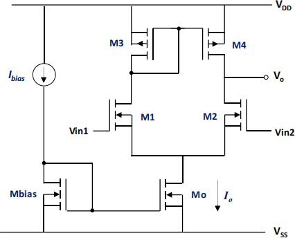
Fig. 1: Circuit design of a single-stage differential CMOS Op-amp.
Typically, the gain obtained from an Op-amp designed using a CMOS technology tends to be lower compared to that developed using bipolar technology. The gain of the CMOS Op-amp can be improved by adding an amplifiers stage such as the common-source stage shown in Fig. 2. Here, the output from the first differential amplifier stage is connected to the second common-source amplifier stage, comprising of apMOST, Mop. The nMOST, Mon is also added and connected to point X. The stability of such an amplifier can also be enhanced by introducing a compensation capacitor (Cc), which is connected between the outputs of the differential and common-source amplifier stages. The value of CC depends on the required phase margin and is typically smaller than CL. For example, for a phase margin of 60o, we can assume, Cc ≥ 0.22 CL .

Fig. 2: Circuit design of a two-stage CMOS Op-amp consisting of a differential stage, common-source stage and compensation capacitor.
The design and simulations of the Op-amp (both single and two stages) will utilise the 1.2 µmCMOS technology on Multisim. With such long channels, we can assume the channel modulation, λ is negligibly small, and thus utilise the standard saturation drain current model. The respective SPICE and design parameters are as specified in Table 1 in Appendix A1, and the design procedures are provided in Appendix A2.
Section 1 - Design and investigate the DC, AC and transient responses of a single-stage Op-amp by simulation and analysis
Design and simulate the single-stage Op-amp in Fig.1 with a voltage gain, Av of greater 100 (> 40 dB), gain-bandwidth product GB of 1 MHz and phase margin of 60o (at unity gain or 0 dB).
a) Calculate the aspect ratios of all transistors (i.e. M1, M2, M3, M4, Mo, and Mbias) in the design. Make sure to represent these as a whole number of λm.
b) Build and simulate the circuit design on Multisim, and obtain the corresponding DC, AC (i.e. Bode and phase plots) and transient (i.e. slew rate, rise/fall edge) responses.
c) Analyse the responses obtained in b), and extract/examine the key parameters from the characteristics including gain, gain-bandwidth and phase-margin etc. Compare and comment on the outputs obtained from the simulations to those provided in the specifications.
d) Further, optimise your design, and show how the gain and gain-bandwidth maybe improved using this design architecture.
Section 2 - Design and investigate the DC, AC and transient responses of a two-stage Op-amp with compensating capacitor by simulation and analysis
Design and simulate the two-stage stage Op-amp in Fig. 2, consisting of an additional common source stage and a compensating capacitor, to operate with a gain, Av of greater than 1000 (≥ 60 dB), gain- bandwidth, GB of 5 MHz, and phase margin of greater than 60o.
a) Calculate the aspect ratios of all transistors (i.e. M1, M2, M3, M4, Mo, Mbias, Mop, and Mon) in the design. Make sure to represent these as whole multiple of λm.
b) Build and simulate the circuit design on Multisim, and obtain the corresponding DC, AC (i.e. Bode and phase plots) and transient (i.e. slew rate, rise/fall edge) responses.
c) Analyse the responses obtained in b), and extract/examine the key parameters from the characteristics including gain, gain-bandwidth and phase-margin etc. Compare and comment on the outputs obtained from the simulations to those provided in the specifications.
d) Further, optimise your design, and show how the gain and gain-bandwidth maybe improved using this design architecture. Comment on the significance of the compensating capacitor.
Section 3 - Investigate amplifier circuits with closed loop gain
In Sections 1 and 2 we investigated the open loop gain of an operational amplifier. In practical applications, operational amplifiers are rarely used as open-loop circuits but is negative feedback to control the gain of the circuit.
a) Briefly explain how negative feedback is used to control gain in operational amplifiers.
b) Modify the circuit from section 1 to build and simulate the circuit design on Multisim, which uses negative feedback to create gains between -0.1 and - 1000, and thus obtain the corresponding DC, AC (i.e. Bode and phase) plots. Explain your circuit and discuss the results. (You probably want to use ‘parameter sweeps’ to automate this – See MultiSim guidance for details).
c) Modify the circuit from section 2 to build and simulate the circuit design on Multisim, which uses negative feedback to create gains between -0.1 and - 1000 and thus obtain the corresponding DC, AC (i.e. Bode and phase) plots. Explain your circuit and discuss the results. Compare with the results from section 3b.
d) Modify the circuit from sections 1 and 2 to build and simulate the circuit design on Multisim, which uses negative feedback to create non-inverting gains between +0.1 and +1000 and obtain the corresponding DC, AC (i.e. Bode and phase plots). Explain your circuit and discuss the results. Compare with the results from sections 3b and 3c.
2024-04-26