CS 251, Winter 2024, Assignment 4
Hello, dear friend, you can consult us at any time if you have any questions, add WeChat: daixieit
CS 251, Winter 2024, Assignment 4
Due Friday, March 1st, 11:59 PM
Accepted until March 6th, 11:59 PM without penalty
1. (12 points)
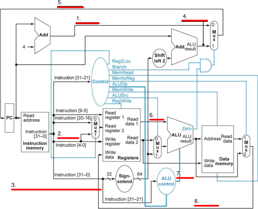
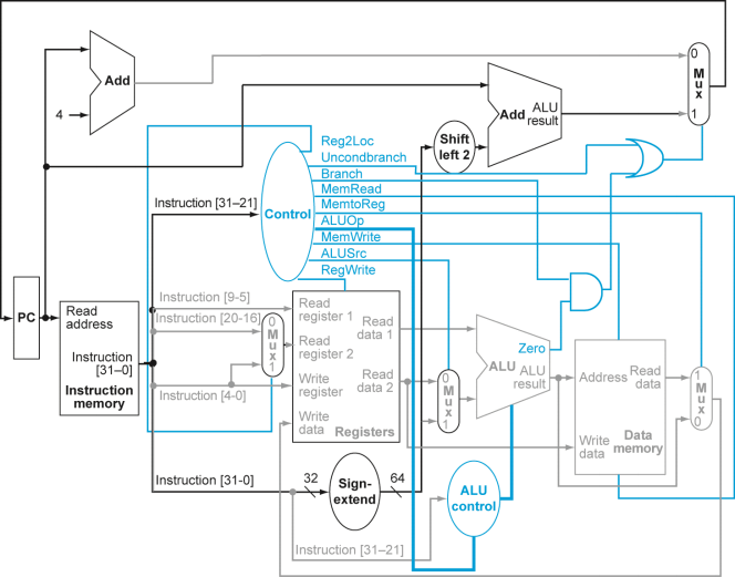
(a) (10 points) Consider the single-cycle computer shown on page 9 of this assignment. Suppose the circuit elements take the following times:
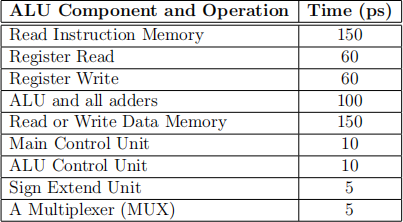
Assume that all other components, PC, Shift Left unit, AND and OR gates take negligible time.
Compute the minimum clock speed required to successfully execute each instruc-tion type below. Show your work.
R-format: ps.
LDUR: ps.
STUR: ps.
CBZ: ps.
B: ps.
(b) (2 points) What should be the length of the clock cycle for this single cycle processor?
2. (9 points)
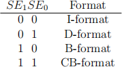
(a) (3 points) I-format, D-format, B-format, and CB-format instructions all have constant fields that get extended to 64-bits. The I-format constant field is treated as an unsigned number, while the other three formats treat their constant field as a 2’s complement, signed number.
Implement the sign-extension unit found in the single cycle datapath. Your sign-extension hardware should take two inputs: the 32-bit instruction A, whose nth bit is referenced as An, and a 2-bit SE input that indicates the format of the instruction:
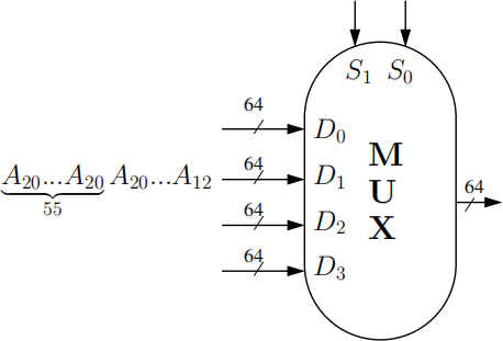
Implement the sign-extension hardware using the 64-bit wide, 4-to-1 MUX shown below. We have completed one of the inputs for you.
Complete the remaining inputs, and be sure to label the input to each select line.
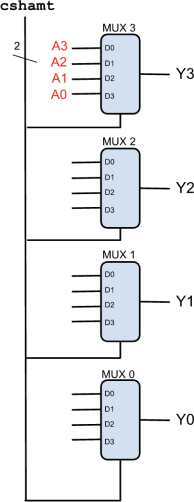
(b) (6 points) Design a 4-bit circular shift left unit using only four (4) 4:1 multiplex-ors. The input A and output Y are 4 bits wide and delineated as A3, A2, A1, A0 and Y3, Y2, Y1, Y0, respectively. Note that the circular shift amount cshamt, is a 2-bit number that enables a circular shift left by 0, 1, 2 or 3 units.
In the figure below, the multiplexors have been arranged to help you design the circular shift left unit.
As an example, we have complete MUX3. If the cshamt = 0, this implies that there is no circular shift, and the output in bit 3 of Y, that is, Y3 should be the same as A3, since A = Y . On the other hand, if cshamt = 1, then input A is shifted left by 1 bit, and Y 3 = A2. Similarly, if cshamt = 2, then input A is shifted left by 2 bits, and Y 3 = A1 and if cshamt = 3, then input A is shifted left by 3 bits, and Y 3 = A0.
Complete the inputs for each of the MUX labelled MUX2, MUX1 and MUX0.
3. (8 points)
Consider the assembly language instruction at memory address 2500:
2500: LDUR X3, [X2, #-18]
In the figure below, there are eight (8) labelled lines in red. On each line, write in the value that travels along the corresponding wire(s) when executing this assembly language instruction.
Note the following requirements and assumptions:
• you should write a number in decimal, binary or hexadecimal, on each dark line, and not an expression involving things like ‘PC’, etc.
Some numbers are more natural to write in binary; for any binary numbers you use, you should subscript them with a ’2’ like 1012.
• Assume that each register Xi (with i = 31) contains the decimal value 200010 + i. For example, X2 contains the value 200210.
• Assume that each data memory cell contains its byte address. For instance, Data Memory at byte address 160 stores 160, that is, DMem[160] = 160.
• Assume that the op field of this D-format instruction is 0.
• Label 2 refers to Instruction[4-0]; Label 3 refers to the 32 bits of the Instruction; Label 7 refers to ALU Control output.
4. (15 points)
Consider the following possible ARM assembly language instructions:
STB X1, [X2,#100]: STB Rd, [Rn,#100] # Store and Branch
ADDW X2, X3, X4: ADDW Rd, Rm, Rn # Add and Write Memory
CBU X2, X3, #10: CBU Rd, Rm, #10 # Conditional branch and update
The STB (store and branch) is an I-format instruction, the ADDW (add and write mem-ory) is an R-format instruction and the CBU (conditional branch update) is an I2-format instruction (discussed below). The effect of each instruction is given below.
STB: MEM[Rn +Immediate] <= Rd; PC <= PC +(4*Immediate)
ADDW: Rd <= Rm+Rn , MEM[Rm+Rn] <= Rm
CBU: Rd <= Rm; If Rm==0 then PC <= PC + (4*Immediate)
When executing on the datapath that handles the B instruction (like the one on page 9 of this assignment), these new instructions do not require any physical hardware changes to the datapath.
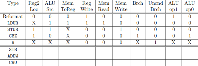
Fill in the table below indicating the value of all existing control lines necessary to execute the STB, ADDW and CBU instructions on the datapath. You must use don’t cares where appropriate.
The STB instruction is similar to the STUR instruction and writes to memory and updates PC to a new address. It stores Rd to memory at the address computed by [Rn + Immediate]. Also, it sets PC to (PC + Immediate×4).
Hint: Even though the STB instruction is an I-format instruction, the main control unit treats it very similar to a STUR instruction. This has implication for the ALUOp control lines.
The ADDW instruction is similar to ADD instruction that computes the value (Rn + Rm) and stores this in Rd. It will also write Rm to Memory at address (Rn + Rm).
The CBU instruction takes the value in register Rm and stores this into Register Rd. Also, if register Rm contains the value zero, PC is updated to P C + Immediate × 4. You may assume for this question that CBU is an I2-format instruction that specifies register Rm in bits 20–16, that specifies the immediate in bits 15–5, and that the Sign-Extend Unit has been extended to handle the immediate in the I2-format. I2-format is given below:

Hint: Even though the CUB instruction is an I2-format instruction, the main control unit treats it very similar to a CBZ instruction. This has implication for the ALUOp control lines.
5. (11 points)
(a) (6 points) Modify the single-cycle computer to handle the Logical Shift Left (LSL) R-format instruction. An example of such an instruction is
LSL X1,X2,#6 : LSL Rd,Rn,Shamt
which computes
R[X1] = R[X2]<<6
i.e., the contents of register X2 are shifted left by 6 (in this example) and stored in register X1. For this question, the shift amount is a 6-bit constant that specifies the number of bits to shift the contents of register Rn to the left. The Rm field is unused and thus is set to 0.
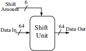
Modify the Single Cycle datapath on the page 9 to handled the LSL instruction. You may add multiplexors, control bits and additional components as needed. You should use the following symbol for the shift left unit:
Be sure that all other ARM instructions executing on the datapath still work. In particular, all other instructions that use register Rn should not shift the contents of register Rn. You may assume that the control unit generates a new signal LSL when the instruction being executed is the LSL instruction.
Summarize your changes to the datapath below, and make the modifications to the datapath provided on the page 9. You may find it convenient to indicate where in the datapath your change will go, and to draw the new hardware in the space below the datapath.
(b) (5 points) In the table below, give the settings of the control bits to implement the new LSL ARM instruction. Use Don’t Cares where appropriate. Make sure you do not break any other instructions. You should be able to determine the purpose and effects of each of the control signals from the Single Cycle datapath on page 9.
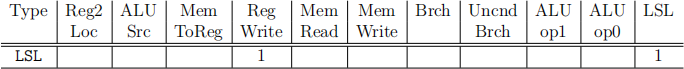
State the value(s) of any new control signal(s) for all other ARM instructions:
6. (12 points)
We want to modify the single-cycle computer to handle the branch and link (BL) instruction. This is a B-format instruction similar to the unconditional branch. An example of such an instruction is
BL #64 ; BL Address
which computes
X30 <- PC + 4
PC <- PC + 64*4
Register X30 is set to PC + 4.
The program counter (PC) is then set to (Address × 4) + PC.
(a) (6 points) Modify the Single Cycle datapath on the page 9 so that BL B-format instruction will work as described above. You may add multiplexors, control bits and additional components as needed. You may assume the the BL instruction will generate a unique control bit.
Marks will also be awarded for the efficiency of the solution. Be sure that all other ARM instructions executing on the datapath still work.
Summarize your changes to the datapath below, and make the modifications to the datapath provided on the next page.
(b) (6 points) In the table below, give the settings of the control bits to implement the new BL ARM instruction. Use Don’t Cares where appropriate. If you need an extra control line to implement this instruction or if you need to increase the number of bits in a control line, add additional columns to the table for the new control line, split a column to increase the number of bits in a control line, and in either case include a note below explaining the effect of the new/increased control line(s) on the datapath and what its setting should be for other instructions. Make sure you do not break any other instructions. You should be able to determine the purpose and effects of each of the control signals from the Single Cycle datapath on the page 9.
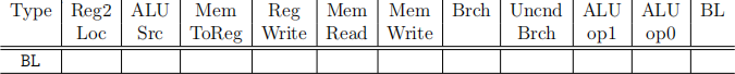
State the value(s) of any new control signal(s) for other ARM instructions:
Single Cycle Processor
2024-03-07