ELEC372/472: Integrated Circuit Design Assignment 2
Hello, dear friend, you can consult us at any time if you have any questions, add WeChat: daixieit
ELEC372/472: Integrated Circuit Design Assignment 2
Objectives:
. To understand the fundamental concepts underlying CMOS gate speed and power performance, as covered in ELEC372/472, in the context of design.
. To simulate, verify and investigate CMOS standard cells using a circuit design package, Multisim.
For guidance, a 15-credit module unit is meant to occupy 150 hours in total (including both private study and contact hours). You should aim to spend about 2-3 hours per week on this assignment.
The remainder of the time will betaken up with background reading and research.
Introduction
Most simulation packages today are based on SPICE (Simulation Program with Integrated Circuit Emphasis) originally developed by the University of California, Berkeley in 1973. It forms the numerical core for most simulation packages and allows to adapt models to particular components. SPICE has a number of advanced MOSFET models developed over a long period of time. In this course, we will utilise Multisim software package which currently supports 10 different CMOS models. For this course, you will utilise a 1.2 µm CMOS technology with respective SPICE parameters as summarised in Table 1 (appendix A). You will need to load the relevant library into MultiSim (see separate instructions).
For assignment 2, you are required to design and investigate the DC and transient responses of a CMOS inverter (details in section 1) and a 2-input NAND gate (details in section 2) by analysis and simulation. You should download the Assignment 2 submission form on Canvas and complete all the sections.
Section 1: Design and investigate the DC and transient response of an inverter by analysis and simulations
Design and test (DC and transient responses) a CMOS inverter as shown in Fig. 1 using the libraries provided. Use an input voltage of 100 MHz 5 V clock source, a supply voltage of 5 V and a load capacitance of 20 fF. For this section, the length of both nMOST and pMOST are set to 2.4 µm, with varying widths as indicated below. Include a printout of the simulation results stating the rise/fall time and overshoot/undershoot.
Instructions for transient and DC simulation are provided in the guidance document.
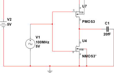
Fig. 1: Set-up of a CMOS inverter circuit.
Investigate a range of different transistor widths as indicated below:
a) pMOST with the width (in microns) equal to the number assigned to you (see the list on Canvas). The nMOST should have a width of 4.8 µm.
b) Set the widths of both nMOST and pMOST equal to the number assigned to you.
c) Set the widths of thenMOST and pMOST devices to be equal to 1.2 µm.
d) Set the pMOST to the width assigned to you and design a matched inverter (where rise and fall times are similar) by adjusting the width of the nMOST. Discuss how you arrived at the
width of thenMOST and how well the design is matching.
e) Discuss the performance of your circuit and how different transistor widths affect it.
f) Discuss what the load capacitance stands for.
g) Sketch a cross-sectional and a top layout view of the CMOS inverter.
h) Explain the physical nature of the contact and active area masks and qualitatively how punch-
though/DIBL/GIDL are affected by reducing the channel length.
Section 2 - Investigate the power dissipation of a loaded CMOS inverter
a) Using your ‘matched design’ from section 1d) and calculate a suitable load capacitance using
your script from assignment 1, employ the ‘power meter’ circuit in the MutiSim guidance,
b) Plot the power dissipation over 5 or more cycles (rise and fall times) of the input signal. Plot input and output voltage waveforms; drain current of p-MOST and n-MOST and power
dissipation of the DUT on the same page but as separate traces.
c) Devise a simulation that allows separation of dynamic power dissipation and short circuit
current power dissipation. Comment on the relative magnitudes of the two components.
d) Repeat the simulation at a lower frequency and compare the results to those of a higher
frequency.
Quote power consumption in both ‘watts’ and as ‘energy per transition’. Check that the values
you are getting are sensible.
Section 3: Design and investigate the DC and transient response of a 2-input NAND gate by analysis and simulation
Design and test (DC and transient responses) a two-input NAND gate as shown in Fig. 2 using the libraries provided with further details below. Use a supply voltage of 5V, an input of 100 MHz 5V clock source and a load capacitance of 20 fF.
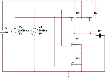
Fig. 2: Set-up of a two-input NAND CMOS circuit.
Investigate the following conditions:
a) The two pMOST widths are to be equal to the number assigned to you and the length of 2.4 µm. The two nMOSTs should have a width of 4.8 µm and a length of 2.4 µm. Perform DC
and transient simulations. Look at any internal nodes as well.
b) Investigate the rise/fall times when the width of both pMOSTs and the widths of each nMOST are varied.
c) Repeat the above and adjust the value of the load capacitance CL to compensate for the different widths of the new transistors. Use your script from assignment 1 to calculate an appropriate load capacitance.
d) Modify thenMOST width to design a ‘matched’ NAND gate.
e) Discuss the performance of your circuit and how different transistor widths affect it.
f) Discuss the influence of the load capacitance on the circuit.
g) In assignment 1, you calculated the capacitance of an inverter, and discuss why this model is still appropriate for aNAND gate.
Appendix A: SPICE Parameters
The parameter values needed for the calculations are as given in Table 1 below:
|
Parameter |
Definition |
NMOS |
PMOS |
|
Vt (V) |
Threshold voltage |
0.79 |
-0.91 |
|
Gamma (V0.5) |
Bulk threshold parameter |
0.5863 |
0.4863 |
|
Phi (V) |
Surface potential |
0.6 |
0.6 |
|
PB (V) |
Bulk potential |
0.8 |
0.85 |
|
Is (A) |
Bulk junction current |
1 × 10- 14 |
1 × 10- 14 |
|
RSH (Ω/sq) |
Sheet resistance |
8.5 × 101 |
1.04 × 10² |
|
*Nsub (cm-3) |
Substrate doping concentration |
2.75 × 10¹⁶ |
1.89 × 10¹⁶ |
|
*NA , ND (cm-3) |
Drain/source doping concentration |
1 × 10²² |
1 × 10²² |
|
CGSO (F/m) |
Gate source overlap |
4.02 × 10- 10 |
5.37 × 10- 11 |
|
CGDO (F/m) |
Gate drain overlap |
4.02 × 10- 10 |
5.37 × 10- 11 |
|
Cj (F/m2) |
Zero bias bulk junction bottom capacitance perm2 of junction area |
3.85 × 10⁻⁴ |
4.84 × 10⁻⁴ |
|
Cjsw (F/m) |
Zero bias bulk junction sidewall capacitance perm of junction perimeter |
1.39 × 10- 10 |
1.65 × 10- 10 |
|
MSJW |
Side grading coefficient |
0.125 |
0.127 |
|
ld (m) |
Lateral diffusion |
1.65 × 10⁻⁷ |
2.2 × 10⁻⁸ |
|
tox (m) |
Gate oxide thickness |
2.12 × 10⁻⁸ |
2.12 × 10⁻⁸ |
|
K (A/V2) |
Transconductance parameter |
9.64 × 10⁻⁵ |
2.94 × 10⁻⁵ |
|
µo (cm2/Vs) |
Surface mobility |
591.7 |
180.2 |
|
XJ (m) |
Junction depth |
0.2 |
0.2 |
|
PS = PD (m) |
Perimeter |
14 × 10-6 |
14 × 10-6 |
|
AS = AD (m2) |
Area |
14 × 10- 12 |
15 × 10- 12 |
Table 1: SPICE parameters for 1.2“m CMOS technology (MOS: Device model level 3).
2024-02-24