EEEE1004: INFORMATION AND SYSTEMS 2023/24 Topic 3 – Semiconductor Devices
Hello, dear friend, you can consult us at any time if you have any questions, add WeChat: daixieit
EEEE1004: INFORMATION AND SYSTEMS 2023/24
Topic 3 – Semiconductor Devices
Coursework 3: Simulation & Design of Diode Circuits using LTspice
Within this coursework, you will again use LTspice, however this time the focus will be on ‘Semiconductor Devices’, more specifically, the simulation and design of diode circuits. There are four questions in total to complete, with the marks for each part shown. Ensure that you carefully follow what you are asked to do and what to include in your document. Your final mark for this assignment will contribute 15% to your final grade for the ‘ Information and Systems’ module. The coursework assesses elements from the ‘Semiconductor Devices Lectures 1-2’ and ‘Seminars 1-2’ with some additional context provided in ‘ Lecture 3’ . In addition to this, for the last part of Question 4, a new diode application is introduced which is only needed for this coursework.
Instructions
You should prepare a single word-processed document with the solutions containing your designed circuit schematics, relevant outputs i.e. graphs or simulation text, and your interpretation of these results when requested. The requested circuit diagrams and graphs must come from your LTspice simulations which you will also be required to submit alongside your document. For any given question, the maximum mark that can be achieved will be 50% if the corresponding LTspice file is not provided. For submission, your document must be converted to a single PDF file. Name this file ‘EEEE1004-CW3-########.pdf’, where ‘########’ is your student ID.
Within your document, number all pages and give your solutions to each question sequentially, making sure it is clear which question and part you are answering. As this is the second coursework involving LTspice, less direction is provided, so you may wish to refer back to the LTspice seminar or feedback from Coursework 2 to ensure that you follow good practice when completing circuit layouts and labelling components. Ensure that you show all of your working out for any calculations, think about the accuracy to which you are quoting values and remember to give appropriate units where needed. Throughout the coursework document, you will be instructed to create six schematics, which should be appropriately named as directed. During each question, you will modify and add to your circuits, but you are only required to submit the final version of each schematic i.e. up to the point before you create the next schematic file.
Submission is via Moodle only – you can find the place to do this on the EEEE1004 Moodle page. Your submission must consist of a total of 7 files: 1 x PDF file and 6 x ASC files from LTspice. The submission box on Moodle will only accept a maximum of seven files and the only permissible types are PDF and ASC – do not try to make and submit a ZIP of your work. Ensure that you click the submit button so that your work is submitted – drafts will not be marked and clicking submit after the deadline will result in a late penalty.
This coursework is an individual piece of work. Please remember your Academic Misconduct training. If you are unsure about what constitutes Academic Misconduct, please ask!
If they are needed, you should use the following values for physical constants in your calculations:
Electronic charge (magnitude): q = 1.60 × 10⁻¹⁹ C
Boltzmann constant: k = 1.38 × 10⁻²³ JK-1
Question 1 [30 marks]
In this question, you will investigate the I-V characteristics of a 1N914 diode. The easiest way to get this component is as follows:
• Use the diode component from the toolbar and place it on your schematic.
• Right click on the diode you have placed and use the ‘Pick New Diode’ option.
• Choose the correct diode from the list.
a) Create a new schematic called ‘EEEE1004-CW3-########-Q1.asc’ and draw a series circuit consisting of a 5V DC voltage source, followed by a 100Ω resistor and then a 1N914 diode. Use the ‘Label Net’ feature to label the voltage across the diode as VD. Remember that in order for LTspice to work, you must always include a ground. Include an image of your circuit schematic in your document. [3 marks]
b) Perform a DC operating point (DC oppnt) simulation and include the copied text from simulation output in your document. From this output, identify the two values that represent the operating point (VQ, IQ) of the diode, i.e. the voltage across the diode and the current through the diode.
Write this operating point in your document, and then use it to calculate:
i. The reverse saturation current, I0, of this diode. Assume n = 1 and T = 293 K.
ii. The static resistance of this diode at its operating point.
iii. The dynamic resistance of this diode at its operating point. Remember: 25/ID [mA].
Show all of your working and answers in your document. [8 marks]
c) Now adjust the DC voltage source so that it performs a sweep of the input voltage from 0V to +10V. Choose an appropriate increment for the sweep voltage. Plot the forward biased diode characteristic and include this plot in your document. [3 marks]
Hint:
You are asked to plot the diode characteristic from the circuit that you have simulated. The diode characteristic is just one line on your graph, and this should be of the diode current, ID, against the diode voltage, VD – not the supply voltage to your circuit. When you first see the plot window after running your simulation, unfortunately the x-axis shows the supply voltage which you have just swept from 0V to 10V. LTspice assumes that this is what you want, but, of course, this is not the case – you want to have the diode voltage on the x-axis. You can change the x-axis to be the diode voltage as follows:
• Right click on the x-axis label.
• A window for specifying the horizontal axis parameters will appear.
• The ‘quantity plotted’ box will say V1 (or whatever name you have given the voltage source which is the supply voltage to your circuit).
• Change the ‘quantity plotted’ to ‘V(vd)’ where ‘vd’ is the net name you gave to the diode voltage. This tells LTspice that you want to plot a voltage ‘V’ which is referenced as ‘vd’.
• You can then add the single trace you need to the plot, i.e. the diode current.
d) Now you will investigate how the diode operating point changes as we move small amounts ‘away’ from the operating point which you have found. Use a cursor on your forward bias characteristic to find values for the diode current, at the following values of diode voltage, where VQ is the diode voltage at your original operating point – as found in b) above:
i. VQ – 10mV
ii. VQ + 10mV
iii. VQ – 50mV
iv. VQ + 50mV
Tabulate the above values of diode voltage (in mV) and their corresponding currents (in mA) in your document. [6 marks]
e) Using the values in your table, calculate the change in current and hence, the dynamic resistance about the original diode operating point for the following diode voltageswings:
i. ± 10mV
ii. ± 50mV
Show all of your working and answers in your document. Compare the two new values of the dynamic resistance, from e) i) and e) ii) above, to each other and then compare them to the value found in b) iii). Comment on any differences. [6 marks]
f) Now adjust the DC voltage source so that it performs a sweep of the input voltage from – 10V to 0V. Choose an appropriate increment for the sweep voltage. Plot the reverse biased diode characteristic and include this plot in your document. From the plot, determine the diode reverse saturation current, I0. Compare this to the value found in b) i) and comment on the potential origins of any differences. [4 marks]
Question 2 [30 marks]
In this question, you will investigate a full-wave, or bridge, rectifier, based on 1N914 diodes.
a) Create a new schematic called ‘EEEE1004-CW3-########-Q2.asc’ and construct a full-wave rectifier. Use four identical 1N914 diodes and a 1kΩ load resistor. Include a voltage source in your circuit, instead of the transformer shown in the lecture, and label this voltage ‘Vin’ . The input voltage should be a 30V sinusoidal signal with a frequency of 1Hz and a DC offset of 0V. Label the voltages at either end of the load resistor as ‘Va’ and ‘Vb’. Include an image of your circuit schematic in your document. [5 marks]
b) Run a transient simulation for 5s. Create a plot with two independent panes that show:
i. the input voltage, Vin.
ii. the voltage output across the load resistor, i.e. the difference between ‘Va’ and ‘Vb’, remembering that this output should be positive.
Include this plot in your document. Explain why the peak voltage of the output is less than peak positive voltage of the input. [6 marks]
Hint:
You are asked to plot the difference between two voltages; which should be called ‘Va’ and ‘Vb’ and placed at either end of the load resistor. You generate such a plot as follows – note that the below instructions assume you want to plot Va-Vb, but you may need to invert this depending on which end of the resistor you have labelled with which label:
• Run your simulation.
• Right click on the plot window and choose ‘Add Traces’.
• Note the box at the bottom of this window that says ‘Expression(s) to add’.
• Click on ‘V(va)’ in the list and it should appear in the ‘Expression(s) to add’ box.
• Type a minus sign in the ‘Expression(s) to add’ box.
• Click on ‘V(vb)’ in the list and it should appear in the ‘Expression(s) to add’ box after the minus sign which you have just typed.
• Click ‘OK’ and you should see your plot with the label ‘V(va)-V(vb)’ at the top.
c) Modify the input voltage so that the amplitude is 3V. Perform another transient simulation that runs for 5s. Create a plot with two independent panes that show the input voltage and the output voltage across the load resistor. Include this plot in your document and then answer the following questions. [8 marks]
i. Estimate the turn on voltage of the 1N914 diode. Clearly explain how you determined your value.
ii. Explain why, in this second simulation, there are significant periods where the voltage across the resistor is zero. Explain why these periods of zero output voltage are much shorter, almost zero, in your first simulation.
d) You will now investigate the addition of a smoothing capacitor in parallel with the load resistor. Experiment with capacitor values of 100µF, 470µF and 2200µF. Include plots of the output voltage (the voltage across the load resistor) for each capacitor value in your document.
For each of the investigated capacitors, use the cursor to determine the ripple of the output voltage. The ripple is defined as the difference between the maximum of the output voltage and the minimum of the output voltage, once it is a periodic signal i.e. ignore the initial charging period of the capacitor. Include a table, in your document, that summarises your values for the voltage ripple, to the nearest millivolt, for each capacitor value. [7 marks]
e) To further reduce the ripple, several capacitors can be used. For a given DC power supply application in this question, the maximum allowable ripple is 70mV. Determine how many 2200µF capacitors need to be implemented in the circuit in order to achieve this. Include an image of your circuit schematic in your document. Also include a plot of the output voltage, making sure that it clear to see that the output voltage ripple indeed meets the specification i.e. think about an appropriate scale for displaying the data. [4 marks]
Question 3 [30 marks]
In this question, you will design several stages to manipulate a 1V sinusoidal input into an output which resembles a 3.3V square wave. The output is then used to drive two light emitting diodes (LEDs) so that both ‘blink’ periodically. Figure 1 shows each stage as well as the approximate ‘ideal’ signal which would be observed at each stage. For this question, you will design each stage in isolation, you do not need to combine the circuits designed in the three parts below.
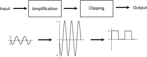
Figure 1: Illustrative Example of Each Stage & the Approximate Waveform Outputted from One Stage & Inputted into the Next
A multi-stage design, such as the one illustrated above, could be used in place of a comparator circuit. The amplification stage must have a significant gain so that once the signal is ‘truncated’ to resemble a square wave, the transition time between the ‘high’ and ‘low’ voltages is minimised i.e. each pulse resembles a square rather than a trapezoidal shape.
Part 1: Light Emitting Diode Circuit [10 marks]
The LED component which you will use for this stage is the ‘QTLP690C’ diode. This can be found using the same method detailed in Question 1.
a) Create a new schematic called ‘ EEEE1004-CW3-########-Q3_Part_1.asc’ and draw a series circuit; consisting of a 3.3V DC voltage source, followed by a 70Ω current limiting resistor and then an LED. Use the ‘Label Net’ feature to label the voltage across the diode as VD and the supply voltage as VS, then run a DC operating point simulation. Include both an image of your schematic and the copied text from the simulation output in your document. [3 marks]
b) Add a second identical branch to your circuit i.e. a second current limiting resistor and LED in parallel with the first branch. Adjust the voltage source so that it outputs a square wave. To do this, right-click on the voltage source → ‘Advanced’ and select ‘PULSE’. Enter the appropriate parameters so that the signal has a minimum voltage of 0V, maximum voltage of 3.3V,no delay time, 0.01ms of rise and fall time,a period of 2msandison for 1ms. Run a transient simulation for 10ms and include a single plot of the voltage across the LED and the supply voltage in your document. Use the cursors to verify that this matches your output in a). [2 marks]
c) Calculate the voltage across the LED, VD, and the voltage across the current limiting resistor, VR
– you must not perform a direct measurement to obtain these values. Verify that these values match the simulation by plotting VS, VR andVD on a single plot and include this in your document
– ensure that the traces are named appropriately. You may reorder the schematic if you require, however you must not add or remove components. [5 marks]
Part 2: Amplification with a Common-Emitter Amplifier [15 marks]
This stage will make use of the ‘2N2222’ bi-polar junction transistor (BJT) to construct a common- emitter amplifier. The easiest way to get this component is as follows:
• Use the componentselection option from the toolbar.
• Choose the device called ‘npn’ and place it in your schematic.
• Right click on the BJT that you have placed and click the ‘Pick New Transistor’ option.
• Choose the correct BJT from the list.
d) Create a new schematic called ‘ EEEE1004-CW3-########-Q3_Part_2.asc’ and place a 2N2222 BJT. Connect the emitter to ground and add separate DC voltage sources to the base and collector. Set the base voltage to 1.6025V, the collector voltage to 3V and perform a DC operating point simulation. Include an image of your schematic and the copied text from the simulation output in your document. [2 marks]
e) Use your circuit and the ‘DC Sweep’ simulation option to generate the input characteristics of the 2N2222 BJT. Keeping the collector voltage at a constant value of 3V, sweep just the base voltage from 0V to 1.5V in increments of 0.01V. Run the simulation and plot the appropriate values; clicking on either the base, collector or emitter end of the BJT will plot the respective current. Include the plot in your document and then use it to determine the BJT threshold voltage. [3 marks]
f) Now use your circuit to generate the output characteristics of the 2N2222 BJT. Replace the base voltage source with acurrent source, ensuring that it is the correct way round, and set the value to 1A. Modify the DC sweep operation so that the first source sweeps the collector voltage from 0V to 3V in increments of 0.01V, and the second source sweeps the base current from 0A to 50µA in increments of 5µA. Run the simulation and plot the appropriate values; include the plot in your document and indicate the saturation, active and cut-off regions. [4 marks]
g) Now the BJTwill be used to construct a common-emitter amplifier, like the one shown in Figure 2 – note that the bypass emitter capacitance has been omitted from this design. Continue to use the 2N2222 BJT and set the resistances as RC = 15kΩ and RE = 1kΩ . Set the input and output coupling capacitances to 10µF and ensure that the resistors and capacitors use the same labels as Figure 2. Use the ‘Label Net’ feature to label the input, output and supply voltages, with the input being a 1V sinusoidal signal with a frequency of 1kHz, and the supply being 30V DC.
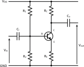
Figure 2: Common-Emitter Amplifier Topology
Determine the appropriate biasing resistor values, R1 and R2, in order to ensure that the current flowing through R2 is ten times greater than the base current of 8.0125µA, whilst VB is 1.6025V. Show all of your working and the complete schematic in your document. [3 marks]
h) Run a transient simulation for 10ms and, on a single plot, show both the input and the output voltage. Include the plot in your document and determine the approximate gain of the amplifier circuit. [3 marks]
Part 3: Clipping with a Diode Clipper Circuit [5 marks]
Clipping refers to a type of waveform distortion that limits the maximum and/or minimum voltages of a signal. Whilst this can be achieved a number of ways, a diode clipping circuit will be used in this question, with voltages above or below a certain level being ‘clipped’ off.
In order to design a diode clipping circuit for voltage waveforms at different levels, a ‘bias voltage’ can be added in series with a diode to produce, what is known as, a ‘combination clipper’. Once the voltage across the series combination of the diode and voltage bias is greater than Vbias + VF, the diode becomes forward biased and conducts.
The orientation of both the voltage source, providing the ‘bias voltage’, and the diode, determines the bias of the diode which, in turn, determines which aspect of the waveform is clipped off. Figure 3, below, shows both a positive bias and a negative bias circuit layout as well as the outputted waveform in each case, assuming VF is 0.7V.
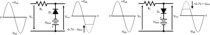
Figure 3: Negative Bias Diode Circuit (left) & Positive Bias Diode Circuit (right) - Note the Vin & VBIAS Orientation
The desired output from the clipping stage should resemble a square wave i.e. the input requires clipping in both the positive and negative halves of the waveform. This can be achieved by combining the two circuits above with different biases; negative voltage values will not be accepted.
i) Create a new schematic called ‘EEEE1004-CW3-########-Q3_Part_3.asc’, and using the 1N914 diode, construct a diode clipper circuit where the output has a minimum voltage of 0V and a maximum voltage of 3.3V – use a resistor value of 1kΩ. The input and output voltage should be labelled ‘Vin’ and ‘Vout’ respectively, where the input voltage is an 11V sinusoidal signal with a frequency of 1kHz. Include the schematic in your document. [2 marks]
j) Run a transient simulation for 10ms and include a single plot of the input and output waveforms in your document. Determine the approximate duty cycle of the output, assuming the threshold between a ‘low’ and ‘high’ state is at 1.65V, showing all of your working. [2 marks]
k) How might a 50% duty cycle be achieved whilst using the same diode clipper circuit? [1 mark]
Question 4 [10 marks]
In this question, you will investigate the properties of various diode types. For each of the four diode types, the following component will be used:
• Silicon Diode: 1N4148
• Schottky Diode: BAT54
• Zener Diode: BZX84C15L
• Light Emitting Diode: PT-121-B
a) Create a new schematic called ‘EEEE1004-CW3-########-Q4.asc’, and place a 1V DC voltage source. In series, add a 100Ω resistor and diode. Do this for all four diodes so that each diode will be series with a 100Ω resistor, and each diode-resistor branch will be in parallel with the others. Add a ‘V_Diode’, ‘V_Schottky’, ‘V_Zener’ and ‘V_LED’ label to the appropriate points in order to measure the voltage across each diode.
Run a DC operating point simulation. Include the schematic in your document and indicate the operating point (VQ, IQ) for each diode. [3 marks]
b) Use your circuit and the ‘DC Sweep’ option to generate the characteristics for each diode. Sweep the supply voltage from 0V to 3V in increments of 0.01V. Generate two plots, the first showing the current through each of the diodes and the second showing the voltage across each diode. Include both plots in your document and determine the forward voltage, VF, for each diode. [4 marks]
c) Comment on the significance of the operating point and breakdown voltage for each diode as well as common applications for each. [3 marks]
2024-02-18