HW1: Semiconductor Fundamentals - Crystal Structures, Band Diagrams, Density of States and Doping
Hello, dear friend, you can consult us at any time if you have any questions, add WeChat: daixieit
HW1: Semiconductor Fundamentals - Crystal Structures, Band Diagrams, Density of States and Doping (100 points)
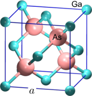
Q1. The semiconductor gallium arsenide (GeAs) adopts the diamond lattice and has a lattice constant of 5.658 Å. It has its valence band maximum at k=0 and its conduction band minimum at the <111>. (30 points)
a) Draw the fcc unit cell and label the [111] direction. (10 points)
b) Calculate the density of GeAS atoms per cm3 . (10 points)
c) Answer: Is GeAS a direct or indirect bandgap semiconductor? (10 points)
Q2. For an unknown semiconductor material, its valence band maximum lies at k=0 and its conduction band minimum lies at <110>. (70 points)
a) Sketch the E vs k diagram for any direct bandgap semiconductor from 0 to the <110> and to the <100>. Label the energy gap (Eg). (10 points)
b) Sketch the E vs k diagram for any indirect bandgap semiconductor from 0 to the <110> and to the <100>. Label the energy gap (Eg). (10 points)
c) Answer: At room temperature for intrinsic samples of Si, ZnO, InP, InAs, and Ge, rank them in order of decreasing conductivity. Explain your answer in 2-3 sentence with reference to the Fermi-Dirac distribution function. (20 points)
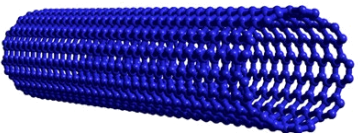
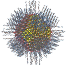
d) For the materials below, draw (by hand) E vs k diagrams and corresponding density of states as shown in slide 35 of lecture 1, Week 1. Hint: You can use Google/internet search or any relevant textbook. Please provide appropriate references in our answers. (30 points)
(i) Semiconducting carbon nanotube
(ii) Bulk crystal GaAs
(iii) CdSe Quantum Dot
2024-01-16
Introduction to Nanoelectronics, Opto-electronics and AI