EECE 7244, Introduction to Microelectromechanical Systems (MEMS) Fall 2023
Hello, dear friend, you can consult us at any time if you have any questions, add WeChat: daixieit
EECE 7244, Introduction to Microelectromechanical Systems (MEMS)
Fall 2023
Packaging Design Problem
Please indicate your makeup strategy:
口 HW makeup: HW #
口 Exam makeup: problem #
Accelerometers are being marketed for consumer applications such as cell phones. The main requirements for accelerometers in this market are low precision and accuracy but in a small-volume, low-profile package. Below is a simplified schematic for an accelerometer. When an acceleration is applied, the comb fingers typically move closer together laterally (in this case, up and down) rather than longitudinally. In actuality, they are fancier than this schematic implies, but for now, this is quite challenging enough.
This exercise will go through several phases to help you understand the fabrication and packaging process. First, we will outline the various options for the fab process and present the device specifications. Then we will outline the various options for the package type. Then, you will go through a series of steps: make a quick assessment of which options are workable, make a plan to release the structure safely, consider the device size constraints, and settle on a detailed process.
Specifications
You will have the option of making a surface micromachined accelerometer, or making one in which the comb fingers are etched out of the device layer of an SOI wafer. No matter what you choose, you need to meet the following specs:
• Totalarea of the capacitors formed by the capacitive fingers: 100,000 μm2
• Mass of proof mass: 3 μg (pSi=2300 kg/m3) ![]() volume of 1.3 x 106 μm3
volume of 1.3 x 106 μm3
• Max area of package: 15 mm2
• Max height: 2.0 mm
• Number of bond pads: 4
• On-chip bond pad size: 50 μmx 50 μm (unless using chip-scale packaging (CSP), in which case use those dimensions)
• Spacing between on-chip bond pads: 50 μm (unless using CSP)
• Packaged device must be tolerant of high temperatures so that it can be safely soldered into the
phone. In other words, the accelerometer must be able to withstand reflow temperatures for flip- chip mounting of packaged device.
• The accelerometer must be packaged in a vacuum environment.
Two fabrication options
There are two main fabrication process flows that you can use as the basis for your packaged accelerometer. One is a surface micromachined polysilicon process, and the other is a bulk-micromachined SOI flow. The processes do not describe how/when to die saw, what the correct mask layout is, and how to vacuum- encapsulate the accelerometer (if desired).

When you sort out your fabrication process flow, you’ll be choosing your parameters (number of fingers, length of fingers, etc) to meet the constraints listed above. For example, to achieve the 100,000 μm2 spec, you could use an SOI wafer with a 20 μm thick device layer and 25 moveable comb fingers that are each 100 μm long. (Then 20 x 100 x 25 fingers x 2 sides of each finger = 100,000). Or you could use a polysilicon surface micromachining process with a 5 μm thick polySi layer and 100 moveable fingers that are each 100 μm long. Or you can come up with your own plan.
Working from your rough plan, you’ll need to assess whether your device will fit into the allotted device area (or rather, whether it will fit inside the package while the package fits into the allotted area). To do this, you’ll need to know how wide your fingers are and how much space is between them. You can assume that the finger width must be at least 1/20th of the finger length (with a minimum width of 2 μm if your fingers are really short), and that your inter finger spacing must be at least 1/5th of your finger height (with a minimum separation of 2 μm if your fingers are really short). Then you can estimate the dimensions of the finger array according to (2wf + 2ws)*Nf.
Packaging options
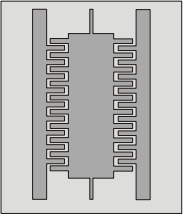
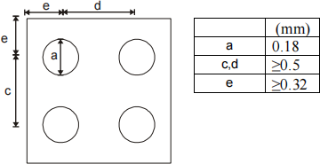
Leadless ceramic chip carrier (LCCC)
• Hermetic: Yes.
• Package thickness: 1.8 mm
• Maximum chip thickness: 800 μm
• Dimensions:
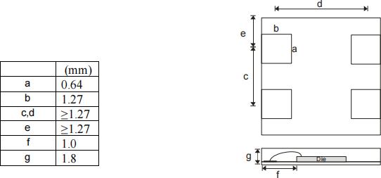
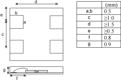
Dual flat no-lead package (DFN)
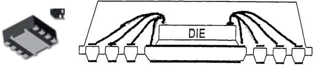
Hermetic: No.
Package thickness: 0.9 mm
Maximum chip thickness: 350 μm
Dimensions:
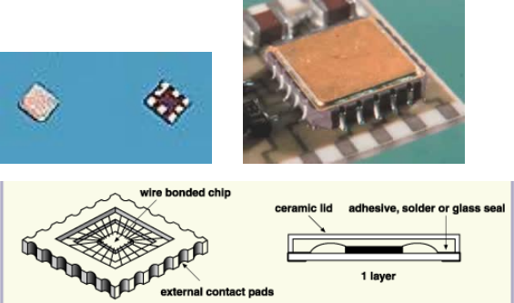
Wafer-level chip-scale packaging (CSP)
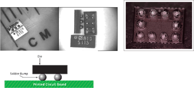
A wafer-level chip-scale package means that you cap off the device with some kind of lid in the fab (think
wafer-bonded),“somehow”get the electrical contacts to the outside of the package on one side or the other, and put solder on it as described below so it can be directly flip-chip bonded. This one is liable to be the smallest option, but it’s also likely to be the most difficult option.
• Hermeticity: Dictated by how the chip is capped off.
• Package thickness: Equal to chip thickness + 100 μm for solder bumps.
• Maximum chip thickness: not applicable
• Note: solder bumps are applied at the wafer level. The wafer must be able to withstand
electroplating of a 5 μm Cu seed layer onto the pads, screen printing a solder paste, and then reflowing the paste at 225 ºC to form bumps.
• Dimensions:
What should you do?
1. (20%) Think through all of the options described in the chart below. Comment on which ones are workable and which are not.
|
|
PolySi surface micromachining |
SOI bulk micromachining |
|
Wafer-level chip-scale packaging |
|
|
|
Leadless ceramic chip carrier |
|
|
|
Dual flat no-lead package |
|
|
2. (40%) Choose one that you’d like to pursue. Brainstorm plans for how to manage die release, wafer separation into dies, and encapsulation into a package that doesn’t involve destroying the fragile released structure. Do the detailed sizing of your accelerometer chip, including the number of comb fingers and the thickness, length, width, and spacing of the comb fingers, being sure to add in room for the bond pads.
3. (40%) Based on this information, design a detailed fabrication process flow and a package process to create an accelerometer that meets the above specs. The most important thing is to try to come up with a complete process that actually works and meets the specs; as a secondary consideration, you should try to think about designing it to make it as small as possible. (Specifically, you want to come up with the smallest volume packaged device that can be mounted on a circuit board.) You’re free to use bulk micromachining or surface micromachining, to start your packaging at the wafer scale or not, etc. You need to consider everything: when the wafer is diced, when the proof mass is released, attachment into the package, etc.
2024-01-13