Computer Hardware and Digital Design Assessed assignment Part 3
Hello, dear friend, you can consult us at any time if you have any questions, add WeChat: daixieit
Computer Hardware and Digital Design
Assessed assignment
Part 3
Introduction
In the first part of the assignment, you created an ALU and a register file. In the second part, you connected them together to form the core of a small microprocessor. In this part you will run a small program on the processor. This will entail resolving timing issues with the instructions. There are a variety of ways to approach this, some of which are simpler and some more complicated. This part should take you the remainder of the lab sessions. When you have finished, you should demonstrate your design working to a PGTA or to Dr. Quigley.
Enabling the register file
The register file that you created is always sensitive to its inputs, even when the inputs have garbage values. This can cause problems because when the simulation initializes (which corresponds to the real hardware being switched on) all the values of the logic signals initializes to some random garbage value (denoted ‘U’ in VHDL, but in real life either a ‘1’ or a ‘0’ chosen at random).
Sometimes it will be necessary to throw away the results of an ALU computation. This will occur when you use a no-op instruction. This should not result in a write back of any value. Give the register file an enable input. When the enable=1 the register file will operate normally. Otherwise the register file will ignore its d_in input, and will not update its contents.
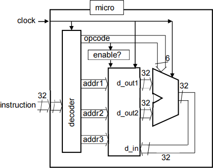
Machine instructions
Machine instructions are supplied to this arrangement in the form of 32-bit numbers. The format of these instructions is as follows:
. The first 6 bits identify the opcode
. The next 5 bits identify first source register
. The next 5 bits identify second source register
. The next 5 bits identify destination register
. The final 11 bits are unused
So, for example, if you want to add the contents of register 1 and register 2 and put the result into register 3, then the machine instruction would be as follows:
. The first 6 bits supply the opcode for the add instruction
. The next 5 bits would address register 1, and the next 5 would address register 2
. The next 5 bits address register 3.
. The remaining bits are unused, and should be set to zero.
The enable signal to the register file should go high when the opcode contains a valid value ALU opcode, and should be low for a no-op or an invalid value.
Test out your design by supplying a sequence of two or three machine instructions to it, and check that the operations performed are correct. Make sure you understand the timing of instructions, and in particular the relationship between the clock cycle on which the instruction occurs, and the clock cycle on which the appropriate result is written to register.
Running a program
Now create a stream of machine instructions that will act as a small program. The program must act as follows:
If the third-from-last digit of your student ID is 1, 4 or 7:
The values stored in the first three registers (1,2,3) should be added to the total, the next three registers (4,5,6) should be subtracted from the total, the next three (7,8,9) added, and so on, i.e.:
total=r1+r2+r3-r4-r5-r6+r7+r8+r9-r10-r11-r12+r13+r14+r15-r16-r17 …
-r18+r19+r20+r21-r22-r23-r24+r25+r26+r27-r28-r29-r30.)
The total should be stored in register 31 at the end of the program. The values of registers 1-30 should not be altered by your program, but the value of registers 0 and/or 31 may be over-written if you wish.
If the third-from-last digit ofyour student ID is 2, 5 or 8:
The values stored in the first five registers (1,2,3,4,5) should be added to the total, the next five registers (6,7,8,9,10) should be subtracted from the total, the next five
(11,12,13,14,15) added, and so on, i.e.:
total=r1+r2+r3+r4+r5-r6-r7-r8-r9-r10+r11+r12+r13+r14+r15-r16-r17 …
-r18-r19-r20+r21+r22+r23+r24+r25-r26-r27-r28-r29-r30.)
The total should be stored in register 31 at the end of the program. The values of registers 1-30 should not be altered by your program, but the value of registers 0 and/or 31 may be over-written if you wish.
If the third-from-last digit of your student ID is 0, 3, 6 or 9:
The values stored in the first two registers (1,2) should be added to the total, the next two registers (3,4) should be subtracted from the total, the next two (5,6) added, and so on, i.e.:
total=r1+r2-r3-r4+r5+r6-r7-r8+r9+r10-r11-r12+r13+r14-r15-r16+r17+ …
+r18-r19-r20+r21+r22-r23-r24+r25+r26-r27-r28+r29+r30.)
The total should be stored in register 31 at the end of the program. The values of registers 1-30 should not be altered by your program, but the value of registers 0 and/or 31 may be over-written if you wish.
You should try to make your program as efficient as possible.
Synchronising the data
All parts of the design that are synchronized to the clock should use only the rising edge of the clock. If you use both the rising edge and the falling edge, then it’s much easier to do the design in simulation, but the real life hardware would be very expensive and complicated to manufacture. You will therefore lose a substantial number of marks if you use both edges of the clock.
One of the main challenges in this design is figuring out on which clock cycle inputs should arrive, and outputs should become valid. If you find that you need to insert registers into some parts of the datapath to get good synchronisation, feel free to do so.
No ops
You may find it useful to create a no-op instruction, i.e. an instruction that instructs the microprocessor to “do nothing” for the next clock cycle, and allocate one of your un-used opcodes to this instruction.
If you don’t manage to finish
Don’t panic. Obviously you will lose marks for having an incomplete design, but you can still achieve a pass mark provided that you do a good write up of the parts that you have finished. The important point to bear in mind is that your report must convince the reader that some parts of the design worked correctly, even if the whole thing does not.
Advanced technical achievement
The main difficulty is finding ways to stop your data being corrupted by pipeline hazards (situations where the data that is needed by one instruction has not yet been finalised by a preceding instruction). There are some simple ways to solve this (for example using no-ops, see unit 7.3), which end up costing clock cycles. These will get you a reasonable mark, but if you are aiming for a high mark then you will need to do better. High marks for technical achievement will be associated with taking measures to ensure that your design has a high throughput (ideally one instruction per clock cycle) without data corruption due to data or control hazards. You can find more detail about this in unit 7.4. An even better (but much harder) approach is to design a processor that can automatically re-order the instructions as they arrive so as to remove problems. You can find more detail in section unit 7.4.
High marks will be gained for managing all of the following:
. correctly describing what features of the problem give rise to hazards,
. demonstrating how they can be solved by software means (re-ordering instructions, using no-ops and using the spare register, 2), and
. separately demonstrating how the hardware can be modified to produce a hardware resolution to the hazards by methods such as register forwarding.
Writing up the assignment
The assignment should be written up as a brief report, which should explain (in about 7-15 pages)
. The ideas behind your design and how it works (in particular what happens on what clock cycle and why);
. How you tested it and how you interpreted the results of your tests;
. Which parts work correctly.
.
Your VHDL code should be included as appendix 1
Print outs of your simulation results should be included as appendix 2 (not more than 4 pages; if you have a large number of results, then you should choose only the most meaningful results, and explain in the text what their significance is)
Deadline and hand-in procedure
The deadline for submission is 12:00 on Tuesday 16th January (week 1of semester 2) using online submission through Canvas.
Collaboration
You are allowed to complete this assignment either as an individual or working in a pair. However, the report must be an individual effort. Also, the opcodes, register file contents and program used must be the ones dictated by your student ID, not those of any other student. If your code has been produced in co-operation with a lab partner, then in your report you should give the student ID (not name) of the person with whom you have co-operated.
Mark scheme
Style, structure and presentation of report 10%
Description of design and testing process 20%
Technical achievements in design, implementation and evaluation 50%
Quality of code (good comments, clear layout, good coding style, meaningful signal and entity names) 20%
2024-01-13