Computer Hardware and Digital Design Assessed assignment Part 2
Hello, dear friend, you can consult us at any time if you have any questions, add WeChat: daixieit
Computer Hardware and Digital Design
Assessed assignment
Part 2
Introduction
In part 1 we started the design of our microprocessor by creating this simplified system.
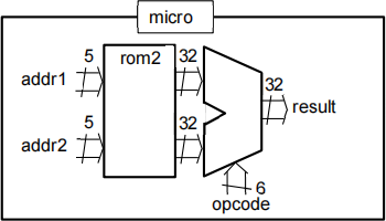
The memory contains 32 different locations, each of which can hold one variable. If, for example, we want to add two variables together, we supply the opcode for “add” and the addresses of the two variables. The sum of the values at those two memory locations will then appear at the “result” output.
In this lab we add features to the system to provide the functionality of a microprocessor processing ALU instructions.
Introduce a clock
Introduce a clock into your system and make the ALU and the memory synchronise to the clock:
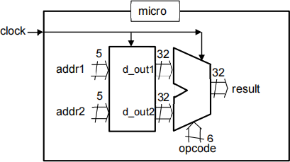
On the rising edge of the clock:
the ALU outputs its response to the opcode and operands that appear at the inputs.
d_out1 produces the item within the register file that is address by addr1.
d_out2 produces the item within the register file that is address by addr2.
Produce a simulation to show the design working correctly.
Introduce a write port into the register file
So far we have given our register file memory two read ports, so we can read out stored values but have no way to change the stored data. Now introduce a write port into the memory. The value appearing at d_in is written into the location referenced by addr3.
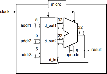
Produce a simulation to show the design working correctly.
The microprocessor
The basic microprocessor has the following appearance:

The microprocessor receives a sequence of machine instructions that are coded as 32-bit words. The format of these instructions is as follows:
The first 6 bits identify the opcode
The next 5 bits identify first source register
The next 5 bits identify second source register
The next 5 bits identify destination register
The final 11 bits are unused
The decoder unit splits the instruction into its required components to feed to the ALU and the register file.
Create the configuration shown in the diagram. Create a machine instruction whose purpose is to add the contents of register 4 and register 5 and to put the result into register 1. Use simulation to show the instruction correctly working.
2024-01-12