ENT782/EN3802 Coursework Field analysis of a damaged microstrip and resonant transmission line
Hello, dear friend, you can consult us at any time if you have any questions, add WeChat: daixieit
ENT782/EN3802 Coursework
Field analysis of a damaged microstrip and resonant transmission line
October 2023
Coursework schedule
Coursework 1 is set in week 3 and is assessed in week 8 via an in person ‘demonstration. ’
Resources
• COMSOL model files
i. ‘Microstrip_lab_timedomain.mph ’
ii. ‘Lab2_TLresonator.mph’
• Sections 1, 2 and 3 of the lecture notes
• COMSOL installation guidance (see Learning Central)
• COMSOL installation files (see Learning Central))
Complete parts I and II.
• If you are enrolled on EN3082 complete part 2.9
• If you are enrolled on ENT782 complete part 2.10
Deliverables
In week 8 there will be a demonstration session in which you will be asked about the approach you took to complete the tasks and questions in this document. You will discuss your work in a 10 minute session in which you will be asked about the underlying theory and to explain your results generated using the COMSOL software. You will be marked out of 100, which will be scaled to obtain the 20% component for this part of the module. You should have key results and figures prepared for the assessment for you to refer to.
In the discussion, marks will be given for clarity of explanation and understanding of the underlying theory, with reference to the lecture notes. The marking sheet that will be used is given in Appendix I of this document.
For any of the questions in this document, if you need more space than is provided, please use a separate document or sheet of paper. Some tasks below require you to prepare plots that will aid your answers to questions. You should prepare these in separate documents to avoid having to generate new plots in COMSOL during the assessment.
Please refer to the guidance provided for access to COMSOL.
Part I - Analysis of a damaged microstrip line
Part I covers the following topics:
• Microstrip design
• Finite element modelling of a microstrip
• Time domain analysis of a microstrip fault
Please use section 1 of DS’s lecture notes as a guide to design considerations and a reference for design equations
Brief: By Finite Element Modelling, using the COMSOL software package, you are required to study a defective microstrip line in the time domain.
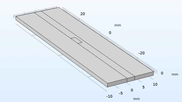
Figure 1: Microstrip line circuit board model using lumped ports. The surrounding air domain is not included for visualization purposes.
Using COMSOL’s RF module, we will simulate a microstrip line. We will then add a discontinuity to represent physical damage, and use ports at each end of the microstrip to analyse signal propagation.
Model Definition
The model describes a 3.3mm wide, 50 Ω microstrip line on a 60 mil (60 mil is 1.524mm) substrate with the dielectric constant of εr = 3.38, and 65mm in length. Later, we will introduce a notch in the middle of the microstrip line to represent an impedance mismatch caused by physical damage, leading to unwanted signal reflections. All metallic parts, including the patterned line on the top of the substrate and bottom ground plane, are set to perfect electric conductor (PEC) by ignoring the loss from a finite conductivity to simplify the modelling process.
![]() The surfaces at each end of the model, bridging between each microstrip end and the ground plane, are used to add lumped ports. The lumped ports excite the microstrip line and terminate it with 50 Ω characteristic impedance. The material on top of the circuit board is air. The exterior surfaces of the air are finished by a scattering boundary condition that is an absorbing boundary to describe an open radiating space.
The surfaces at each end of the model, bridging between each microstrip end and the ground plane, are used to add lumped ports. The lumped ports excite the microstrip line and terminate it with 50 Ω characteristic impedance. The material on top of the circuit board is air. The exterior surfaces of the air are finished by a scattering boundary condition that is an absorbing boundary to describe an open radiating space.
Simulation
1.1 Open the file ‘Microstrip_lab_timedomain.mph’
This is a model of the microstrip line described above. In the Model Builder tree, you will see nodes, each describing a different aspect of the model.
1.2 Expand the ‘Component’ node to explore the model definition. In the Geometry node, you will see a number of blocks, which define the microstrip line, its substrate and the enclosure (which has been hidden from view in the Graphics window).
The ‘Electromagnetic Waves, Transient ’ node describes the physical properties to be studied. Here, we have defined two Lumped Ports to study the signal transmission characteristics of the microstrip.
1.3 If you click on the Lumped Port nodes, you can determine from the Settings pane which of the ports is the input.
The input signal is defined in the Global Definitions nodes near the top of the Model Builder tree. A Gaussian pulse is defined.
1.4 Click on ‘Parameters’ in the Global Definitions node and change the frequency of the pulse to 15GHz.
1.5 Expand the Study 1 node and click on Step 1: Time Dependent. The model will calculate a solution for the electromagnetic fields of our pulse for each time step defined in this node. Note that the array defining the time step is written using the function range(0,T/24,10*T).
The syntax of this function maybe familiar from Matlab and gives a series of equally spaced points from 0 to 10*T,with T/24 between each point. The solution of this study will therefore contain 250 time steps.
1.6 In the settings pane of the Time Dependent study, click ‘Compute’. You will now have to wait a while for the model to be solved.
1.7 Using the design equations from section 1 of the course notes, determine the time taken for a 15GHz signal to travel the length of the microstrip line described above.
Note that when the width of a microstrip line is greater than the depth of the substrate, we can approximate the effective permittivity by
1.8 After solving the Comsol model, select and plot different time steps to examine the evolution of the Gaussian pulse in time. By selecting different time steps and locating the position of the pulse in each case, determine the time taken for the pulse to traverse the length of the microstrip. How does this compare with the result in 1.7 above? Is the pulse Gaussian?
1.9 In the Model Builder tree, click on Geometry>Work Plane 1>Plane Geometry. Right click on Rectangle 1 and click enable from the pop-up menu. Click ‘Build All’. This discontinuity in the metallised microstrip line will act as the physical damage in our study.
Now that the geometry of the physical damage has been drawn, we must change the properties to remove the perfect electric conductor from this small section. In the Model Builder tree, click on Electromagnetic Waves, Transient>Perfect Electric Conductor 2. In the settings pane, select the surface representing the physical damage and remove it from the list to create the discontinuity.
1.10 Now solve the model again, by clicking on Study 1, and clicking ‘Compute’ in the settings pane.
1.11 Click on Results>Electric field 1, then in the shortcuts bar at the top of the screen, click Animation>File.
1.12 In the settings pane, change ‘Number of frames’ to 50 and click ‘Export’ .
1.13 Open the exported .gif file. What happens to the pulse after it reaches the discontinuity? What is the cause?
1.14 By right-clicking on the results node, create a 1D plot showing the power at port 1. How long did it take for the reflected signal to arrive back at the input port? Can you determine the distance to the damage by analysis of signal reflections?
Part II - Analysis of a resonant transmission line
Part II covers the following topics:
• Resonant microstrip transmission line (TL) design
• Finite element modelling of a resonant TL
• Frequency domain analysis of a resonant TL
Please use sections 1, 2 and 3 of DS’s lecture notes as a guide to design considerations and a reference for design equations.
Brief: By Finite Element Modelling, using the COMSOL software package, you are required to study a resonant transmission line.
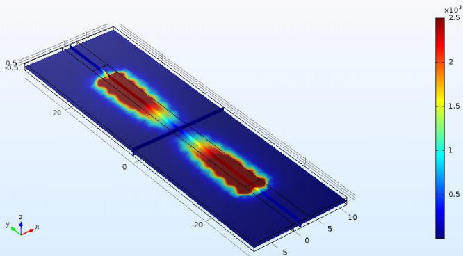
Figure 1: Electric field plot of a resonant microstrip line model using an eigenfrequency analysis.
Using COMSOL’s RF module, we will simulate a resonant microstrip line section. We will then search for resonances using eigenfrequency analysis and examine the effects of coupling on the resonance.
Model Definition
The model describes a 3.3mm wide, 50 Ω microstrip line on a 60 mil (60 mil is 1.524mm) substrate with the dielectric constant of εr = 3.38, and 65mm in length. Two gaps isolate a resonant section in the middle of the transmission line. All metallic parts, including the patterned line on the top of the substrate and bottom ground plane are set to be perfect electric conductors (PEC) by ignoring the loss from a finite conductivity to simplify the modelling process.
The surfaces at each end of the model, bridging between each microstrip end and the ground plane, are used to add lumped ports. The lumped ports excite the microstrip line and terminate it with 50 Ω characteristic impedance. The material on top of the circuit board is air. The exterior surfaces of the air are finished by a scattering boundary condition that is an absorbing boundary to describe an open radiating space.
Method
2.1 Open the file ‘Lab2_TLresonator.mph’
This is a model of the transmission line (TL) resonator described above. In the Model Builder tree, you will see nodes, each describing a different aspect of the model.
2.2 Expand the ‘Component’ node to explore the model definition. In the Geometry node, you will see a number of blocks, which define the TL, its substrate and the enclosure (which has been hidden from view in the Graphics window). Note also the work plane, which is used to define 2D surfaces (in this case, coupling gaps on the surface of the microstrip line).
The ‘Electromagnetic Waves, Frequency Domain ’ node describes the physical properties to be studied. Here, we have defined two Lumped Ports to study the signal transmission characteristics of the microstrip.
2.3 Click on ‘Parameters’ in the Global Definitions node and observe the TL length.
From section 3 of the lecture notes and using the same approximation as in 1.7, use the effective permittivity and the TL length to determine the first three resonant frequencies of the line.
2.4 Expand the Study 1 node and click on Step 1: Eigenfrequency. What is an eigenfrequency? How does Comsol search for eigenfrequencies?
2.5 Use the eigenfrequency settings panel to search for the first three resonances.
2.6 Once you click compute and a list of eigensolutions is given, you will need to look through them and positively identify the three resonances by considering their field patterns and comparing them against the expected field patterns for the resonant modes. Look at the electric field using the expression ‘emw.normE’ in the settings panel of the multislice plot. Change the expression to ‘emw.normH’ to observe the magnetic field. You will be expected to show the E- field and H-field plots for each mode and fully explain their form and their frequencies. Why are the eigenfrequencies given as a complex number? Do the analytical and numerical frequencies match well? What are the causes of any differences?
2.7 Right-click on Study 1 > Step 2: Frequency domain, then click ‘Enable’. By the same method, disable the Eigenfrequency analysis.
2.8 In the settings panel of the Step 2: Frequency domain node, use the ‘range’ button to the right of the Frequencies text box to generate a list of up to 10 frequencies spanning 100 MHz around the first resonant frequency determined in the eigenfrequency analysis above, then compute. What is the impact of changing the frequency? At the resonant frequency, does the resonant mode look the same as in the eigenfrequency analysis? Is the transfer of energy to the resonator effective? Prepare representative plots and be prepared to fully explain your findings.
If you are enrolled on EN3082, do 2.9. If you are enrolled on ENT782, do 2.10.
For EN3082 students only:
2.9 Use the parameter ‘coupling_gap’ to explore different coupling strengths and improve energy transfer to the TL resonator. By noting the peak field in the resonant section, design an optimised gap size to achieve maximum power transfer into the resonator. You will be required to give a full explanation of your design. Generate a 1D plot of the S21 parameter for each frequency to observe the resonance (i.e. S21 vs frequency). Hint: (i) Right-click on the Results node and select ‘1D Plot Group’, (ii) Right-click on the new 1D plot group and select Global, (iii) Select ‘Add expression’, and find S21 in dB in the Ports sub-menu. Compare the resonant Lorentzian peak to the examples in the lecture notes (you may need to simulate more frequency points). Can you tell if the resonant TL is overcoupled or undercoupled? What is the fraction of power transferred at resonance?
For ENT782 students only:
2.10 Use the parameter ‘coupling_gap’ to explore different coupling strengths and improve energy transfer to the TL resonator. By noting the peak field in the resonant section, design an optimised gap size to achieve maximum power transfer into the resonator. Provide a full explanation of your design. This is an example of ‘end coupling’. What other planar coupling structures are available? Are they appropriate here?
Generate a 1D plot of the S21 parameter for each frequency to observe the resonance (i.e. S21 vs frequency).
Hint: (i) Right-click on the Results node and select ‘1DPlot Group’, (ii) Right-click on the new 1D plot group and select Global, (iii) Select ‘Add expression’, and find S21 in dB in the Ports sub-menu.
Compare the resonant Lorentzian peak to the examples in the lecture notes (you may need to simulate more frequency points). Can you tell if the resonant TL is overcoupled or undercoupled? Depending upon the load, the coupling strength may vary during operation, for example with temperature. How can you design a variable coupling that can be adjusted during operation to ensure that maximum power transfer is maintained? Provide full details of your solution and any references you use.
Bibliography
‘Transmission Lines and Waveguides’, EN3082/ENT778 Section 3 HF RF Engineering course notes, D R Slocombe, Cardiff University, 2023
‘A Designer's Guide to Microstrip Line’, I. J. Bahl and D. K. Trivedi, Microwaves, May 1977,pp. 174- 182.
‘Transmission Lines and Waveguides’, EN3082/ENT778 Section 1 HF RF Engineering course notes, D R Slocombe, Cardiff University, 2023
‘Study of a Defective Microstrip Line via Frequency-to-Time FFT Analysis’
‘A Designer's Guide to Microstrip Line’, I. J. Bahl and D. K. Trivedi, Microwaves, May 1977, pp. 174- 182
Appendix I – Demonstration marking sheet
|
Student name: |
Examiner’s Initials |
|
Date: |
|
ENT782/EN3082 CW1 DEMONSTRATION
1. Understanding of the purpose/relevance of the exercise. What are the main conclusions? [20%] /20
2. Understanding of background/theory [40%] /40
3. Understanding of the method [20%] /20
4. Design approach [20%] /20
Mark /100
2024-01-12