EENG20400 Digital Systems 2023/24
Hello, dear friend, you can consult us at any time if you have any questions, add WeChat: daixieit
School of Electrical, Electronic and Mechanical Engineering
EENG20400 Digital Systems 2023/24
Logic Minimisation
1. Use K-maps to find a minimum SOP (sum of products) circuit and a minimum POS (product of sums) circuit for each of the following functions:
(a) f(A,B,C, D) = Σm(0, 2, 3, 4, 5, 6, 8, 11, 12, 13)
(b) f(p,q,r, s) = Σm(0, 1, 5, 7, 8, 9, 12, 14, 15) + Σd(3, 11, 13)
(c) f(x1 , x2 , x3 , x4 ) = Σm(0, 2, 3, 4, 5, 6, 7, 8, 11, 12) + Σd(9, 13)
2. Optimize the following fuctions that are given in maxterms into POS and SOP forms:
(a) f(x1 , x2 , x3 , x4 ) = ΠM(2, 5, 6, 7, 8, 9, 10, 11, 14)
(b) f(x1 , x2 , x3 , x4 ) = ΠM(5, 7, 9, 11)
3. Enter the function f(A,B,C, D) = Σm(0, 2, 8, 9, 10, 12, 13) on a three-variable K-map using D as the map-entered variable. Consider how the function might be minimised using this map and check your answer by minimising the corresponding four-variable K-map.
4. The diagram shows an implementation using multiplexers of a combinational function f(A,B,C,D). Deduce an expression for the function as a sum of minterms.
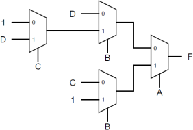
Figure 1:
5. A truth table for logic functions f1 and f2 are given as:
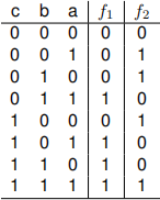
Implement f1 and f2 functions using VHDL behavioural constructs. Draw the corresponding synthesis result.
6. Use a K-map to find a minimal sum-of-products for: f =AB¯ ¯+CD¯+ABC +AB¯ ¯CD¯+ABC¯D+ACD¯ ¯ ¯.
7. (a) Use an 8-to-1 multiplexer to realize the function f(a,b,c,d) = Σ(1, 2, 3, 4, 5, 6, 8, 11, 15) with a,b and c as the control inputs.
(b) Use a 4-to-1 multiplexer and any extra logic gates you may need to implement the function of part (a). Use variables c andd as the control inputs to the multiplexer.
Modelling Combinational Logic Circuits
1. Write a behavioural VHDL module that takes in two two-bit numbers and outputs the product of the inputs.
How would you use this design entity to develop a two 4-bit number multiplication?
2. Design a VHDL module, isprime, to identify whether a given 4-bit number is a prime or not.
3. A 3-to-8 decoder can be described by the following truth-table (in and out are the input and output respectively.)

Design a VHDL module to model this function.
4. Write a VHDL module that takes a five-bit input and outputs a five-bit value that is equal to the input with its bits reversed. For example, input 01100, gives output 00110 and input 11110 gives output 01111.
5. Barrel Shifter: Design a shifter circuit which can shift a four-bit input vector, A, one bit-position to the right when the control signal Right is equal to 1, and one bit-position to the left when the control signal Left is equal to 1. When Right = Left = 0, the output of the circuit should be the same as the input vector. Assume that the condition Right = Left = 1 will never occur.
6. Design a VHDL module to count number of ones (1’s) in a bit string. If the input is 11011012, the output should be 1012.
7. Design a digital circuit that converts a 8-bit Celcius temperature value to its equivalent Fahrenheit value using F = ![]() C + 32
C + 32![]() ≈ 2, but it is very crude. Also,
≈ 2, but it is very crude. Also, ![]() ≈ 1 +
≈ 1 + ![]()
![]()
![]()
![]() = 1.796875
= 1.796875
8. In order to display a number larger than 9 using seven-segment display, the number should be sepa- rated into its digits representing 1’s, 10’s, 100’s and so on. This can be achieved by dividing number by 100 to find hundreds, then the remainder by 10 to find the tens, etc ...
In this task, to convert a binary number into separate binary numbers representing digits of the dec- imal number, we use Double-Dabble Algorithm. The algorithm is explained in Table 1 using an ex- ample. In the table there are three columns showing the 100’s, 10’s and 1’s of the number and the number to be displayed is on the forth column. Last column explains the operation carried out. The algorithm is as follows:
(a) Shift all bits in the number to the left by one bit position.
(b) If any column (100’s, 10’s, 1’s, etc.) is 5 or greater, add 3 to that column.
(c) If 8 shifts have been performed, it’s done! Evaluate each column for the BCD values. (d) Go to step 1.
Why Double-Dabble Algorithm is better than finding hundreds, tens and ones using divisions?

Table 1: Double-Dabble Algorithm Example
Modelling Sequential Logic Circuits
1. (a) A toggle flip-flop (TFF) complements its state (stored value) when its input (T) is ’1’. It retains its state when the input T is ’0’. How would you model this in VHDL?
(b) Consider the circuit in Figure2. It is a 4-bit synchronous counter which uses four T-type flip-flops. The counter increments its value on each positive edge of the clock if the Enable signal is high. The counter is reset to 0 on the next positive clock edge if the synchronous Clear input is low. You are to implement a 8-bit counter of this type.
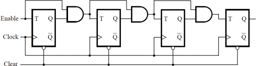
Figure 2: Counter circuit using T-type flip-flop
Write a VHDL file that defines an 8-bit counter by using the structure depicted in the figure. Your code should include a T flip-flop moudle from part a that is instantiated 8 times to create the counter.
2. Draw a timing diagram for the following circuit.
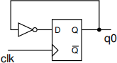
3. Consider the following feedback circuit constructed using a D flip flop:
Plot the output(q0) waveform for the following clk and input sequence (x). Assume initial state is q0 = 0

4. Write a VHDL module that implements the following circuit. Exact syntax is not important.
5. In the sequential circuit shown in Figure 3, the timing parameters for the gates and flip-flops are as follows:
Inverter: tpd = 0.01ns
XOR Gate: tpd = 0.04ns
Flip-flops: tpd = 0.08ns,ts = 0.02ns,th = 0.01ns
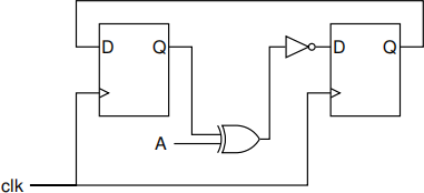
Figure 3: Flip-flop circuit
Determine the maximum frequency of operation of the circuit.
6. Design a 8-bit counter circuit given in the figure below:
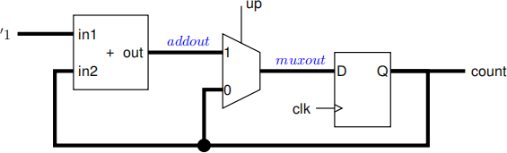
Figure 4: Counter Circuit Schematic
Finite State Machines (FSMs)
1. Determine the state and the output values generated by the state machine in Figure 5 for the input bit sequence given in the table below:

Figure 5: State Diagram for Q2
2. A welding plant is to be automated and its assembly line is going to use a robot welder. Each item to be welded requires seven welds in a strict sequence. The output of the welding control unit for the seven welds is a 3 bit-code is the sequence: 001→ 101 → 111 → 100 → 110 → 010 → 011. The units to be welded are on a continuous feed system. Detectors are activated each time the unit is in the correct position to be welded. You are required to design this control unit.
3. A sequential circuit has two inputs, w1 and w2, and an output, z. Its function is to compare the input sequences on the two inputs. If w1 = w2 during any four consecutive clock cycles, the circuit produces z = 1; otherwise, z = 0. For example
w1: "0110111000110”
w2: "1110101000111"
z : "0000100001110"
Draw a state-machine for this behaviour.
4. A given FSM has an input, w, and an output, z. During four consecutive clock pulses, a sequence of four values of the w signal is applied. Derive a state graph for the FSM that produces z = 1 when it detects that either the sequence w : 0010 or w : 1110 has been applied; otherwise, z = 0. After the fourth clock pulse, the machine has to be again in thereset state, ready for the next sequence.
5. The transmitter of a secure military communication system is transmitting a continuous string of pseudo random zero-one pattern. The receivers in the field are constantly monitoring the incom-ing data sequence for two consecutive one’s that indicate possible arrival of a valid data packet. A valid packet of data contains five bits and no more than three 1’s including a leading pair of 1’s. This synchronous receiver has one input and one output that goes from “0” to ‘1’ whenever the last string of five bits of a packet contain exactly three 1’s and started with two consecutive leading 1’s. Note that a bit before a packet must be a zero, see the example. Analysis of the next packet of data will not start until the end of the previous packet of five, whether it produces a ‘1’ output or not. For example:
input sequence: "00010110101011001011100”
the output generated: "00000000010000001000001”
Design a state-graph/ASM diagram to describe this behaviour.
6. A simple electronic lock system has two external inputs provided by two keypad switches (x1 and x2). The switch inputs are normally logic “0”. When either of the two switches is pressed, the appropriate input will change from “0” to “1”. The single output (z) of the machine is connected to a coil circuit of an electromagnetic lock. The coil will only energise and open the lock (z=’1’) when the correct number sequence “00”, ”01”,”10”,”11” is applied to the inputs (x1x2). Construct a Mealy type state diagram that describes the operation of this circuit.
7. A synchronous controller has one input (X) and one output (Y). This input is connected to a channel to identify two 4-bit code sequences from two sensors. When the input sequence 1001 or 0101 occurs, an output of two successive 1s will occur. The first of these 1s should occur coincident with the last input of the 1001 or 0101 sequence. The controller will start identifying the codes when the second 1 output occurs. For example:
input sequence: 01101100010010110101001011
the output generated: 00000000000011000001100011
8. Design a sequential distress receiver system that acts as a pattern recogniser. At the receiver input this information arrives as a continuous random stream of bits (“0”s and “1”s). A distress signal in the incoming sequence of bits constitutes at least a group of THREE consecutive “1”s, which means “111” .
This system has one input and one output. The output of the system will go to “1” as soon as a group of at least four “1”s had been detected at the input.
The receiver has a memory which keeps last three bits of the information received and it will make the decision at the arrival of the 3rd bit whether the pattern constitutes a distress call or not. When the system is first turned on the values in the memory will be “00” . For example, at the start, with an arrival of ‘1’ the memory will be updated with “01” as the new value. If a “0” arrives next, the new memory will be “10” .
9. Design a sequential distress receiver system that acts as a pattern recogniser. At the receiver input this information arrives as a continuous random stream of bits (“0”s and “1”s). A distress signal in the incoming sequence of bits constitutes at least a group of THREE consecutive “1”s, which means “111” .
This system has one input and one output. The output of the system will go to “1” as soon as a group of at least four “1”s had been detected at the input.
The receiver has a memory which keeps last three bits of the information received and it will make the decision at the arrival of the 3rd bit whether the pattern constitutes a distress call or not. When the system is first turned on the values in the memory will be “00” . For example, at the start, with an arrival of ‘1’ the memory will be updated with “01” as the new value. If a “0” arrives next, the new memory will be “10” .
10. Two digit Binary Coded Decimal (BCD) number is entered into a circuit as a 8-bit binary string, for example the decimal number 73 is encoded as 01110011, first four digits represents 7 and the last four, 3. You are required to design a circuit to convert this binary string to equivalent binary number. When the input is 01110011, the output is: 01001001. Design a digital circuit in VHDL to perform this function.
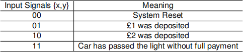
11. Design a sequential controller for a toll collector machine. The machine accepts £1 and £2 coins and the correct toll is £3. If no payment is received within a specific period of time the machine will issue a reset signal to the controller and any money so far is lost. The machine has two outputs. One is Light (L) that is either green (“1”) or red (“0”). The light becomes green if the coins total or exceeds £3. The other output is an Alarm that rings (“1”) a bell as a car passes the red light without full payment. The control system has two external inputs “x” and “y”, the behaviour of which is described below.
Construct a State Graph or State Chart that describes the operation of the toll collector system.
12. The ABC Widget Company manufactures widgets that are required to be of a specific minimum length. The Company wishes to automate the sorting of these widgets by passing them through a tube containing two sensors. These sensors are separated by the required minimum distance. A sensor is activated when a widget is above it. If a widget is too short then it must be rejected by opening the trapdoor. If a widget is long enough then it will continue to travel along the tube (See figure below). You are required to design a state machine that identifies when a widget is too short and activates the trapdoor motor in order to reject the widget. Your control unit is also responsible for closing the trapdoor after rejecting a widget. You may assume that (If you make any other assumptions, you must declare them):
• there is sufficient time to open the trapdoor after the widget clears sensorb,
• the next widget will not arrive over sensora before the trapdoor has had time to close, and
• there are sensors to indicate when the trapdoor is fully open and fully closed.
13. A company has commissioned you to design a synchronous sequential controller for its car park that can accommodate 32 vehicles. The car park system comprises of:
• Opto-electronic sensors at the entrance and exit of the car park
• An up/down counter and associated circuitry,
• A control signal to operate the barrier at the entrance, and
• A signal to illuminate the “FULL” notice at the entrance as required.
When the car park is full, the “FULL” sign should illuminate, and the barrier should remain down until spaces become vacant. Construct an ASM diagram to describe this behaviour.
14. Your task is to design an automatic door control system which has three inputs PD, DO, and DC generated by external sensors and two outputs M and OPN.
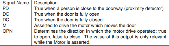
The control algorithm must satisfy the following constraints:
• Opening is initiated whenever a person is detected near the doorway.
• Once fully open, the door may start to close provide condition (a) is satisfied.
• The door must not be driven beyond its fully open or fully closed position.
What is the best diagram to describe this behaviour?
Digital System Design
1. The factorial of a number n is defined as n! = 1×2× ... ×n). This can be expressed as an algorithm which is shown below:
n ⇐ a in ;
p = 1 ;
while ( n > 1 ) {
p = p * n ;
n = n −1;
}
Output ⇐ p ;
Design a processor architecture for this algorithm. You do not need to write VHDL code for this.
2. Integer division of two numbers A and B can be easily
Q = 0 ;
R = A ;
while (R − B > 0 ) {
R = R − B ;
Q = Q + 1 ;
}
Design a processor architecture for this algorithm. You do not need to write VHDL code for this.
3. In an Ulam sequence ui for any positive non-zero integer u0 as the initial value, the element ui+1 of the sequence is computed from its previous element ui, recursively, according to the following rules: 1. If ui is 1,then stop
2. If ui is even, thenui+1 = ui/2
3. If ui is odd, thenui+1 = 3ui+ 1
4. Continue with this process until reaching 1.
Mathematician Stanislav Ulam proposed that any positive integer would reduce to 1 if the above rules were repeated a sufficient number of times. For example, if the original number were 13, the algorithm would generate the following sequence of numbers: 13, 40, 20, 10, 5, 16, 8, 4, 2, 1. This
Ulam sequence has 10 numbers including the original number and the 1.
How would you design this circuit?
2024-01-10