VLSI Design -- Fall 2023 Laboratory Exercise 2
Hello, dear friend, you can consult us at any time if you have any questions, add WeChat: daixieit
VLSI Design -- Fall 2023
Laboratory Exercise 2
Due: Nov/22/202023.
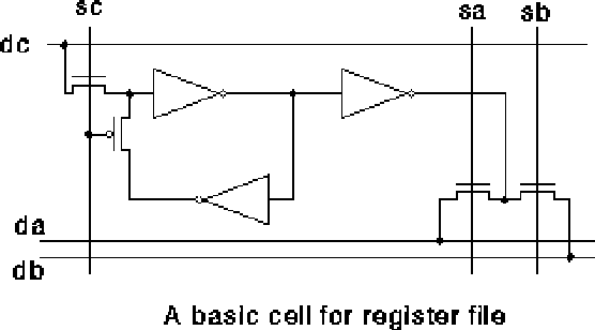
The figure below gives the schematic for a register cell with one input port and two output ports (with control lines for each port)
Operation of the register cell
The memory cell consists of three data lines, a data in (dc) and two data out (da, db) lines. There are three controls, Write (sc), Read A (sa), and Read B (sb). Note that the data and control lines need to pass from one end of the cell to the other so that multiple cells may be connected together to produce a register array. The core of the memory cell is the two inverters connected back to back with the p-channel transistor. This transistor is on when sc is 0, so the information stored in the cell just circulates through the two inverters. When sc is 1, the feedback loop is broken, and the Write input dc is connected (through the n-channel transistor) to the input of the first inverter, forcing the logic value on dc to be stored in the cell. The third inverter serves as a buffer for the cell, and produces the correct logic value when the cell is read. The controls sa and sb turn on the appropriate n-channel transistors, putting the logic value on the respective output lines.
Steps to be performed in the lab
1. Design the schematic using Sedit of the four bit register.
2. The Layout using Ledit for the the basic cell and verify the design.
3. Simulate it with various sequences to check correctness.
4. Does this design suffer degradation in signal voltage levels.
Grading/Submission
For the successful completion of lab1 the grading procedure shall require you to:
2. Turn printouts of the following.
a) The final Schematic of the of the four bit cells.
b) The final layout of the basic one bit register cell.
b) Simulation traces for the sequences used to verify the correctness of the design.
2023-12-20