2ND YEAR DIGITAL SYSTEMS DESIGN LABORATORY 2023/24
Hello, dear friend, you can consult us at any time if you have any questions, add WeChat: daixieit
Department of Electrical Engineering and Electronics
2ND YEAR DIGITAL SYSTEMS DESIGN LABORATORY 2023/24
LAB SESSION #2
Introduction
In the previous lab session we learned how to create module descriptions of simple combinatorial logic circuits in VHDL, and simulate them to verify the behaviour. In this session we will examine sequential logic, more elaborate test bench techniques, and instantiation of IP blocks (“black boxes”).
There are four marked coursework assignments, that can be completed before, during or after the lab session, by the specified deadline. The details of your individual assignments can be found in the on-line DSD2 Coursework System, under the Laboratory 2 tab. The submission of the assignments is done electronically, using the on-line DSD2 Coursework System.
The coursework assignments associated with this lab are marked as follows:
Assignment 1 – 1 mark
Assignment 2 – 2 marks
Assignment 3 – 3 marks
Assignment 4 – 4 marks
In total, these assignments are worth 10% of your final DSD2 module mark
Submission deadlines for each assignment, and maximum marks available in each assignment, are shown on the DSD2 Coursework System webpage.
You are allowed multiple submissions. You may be able to improve your mark in any of the assignments that were awarded less than maximum marks if you submit a revised solution. The maximum mark in any of the assignments is available for the first submission of each assignment. Each subsequent submission has the maximum possible mark reduced by 30% (i.e. it falls-off exponentially: 100%, 70%, 49%, 34.3%, etc. - so that you will always gain some marks if you submit a correct solution). Your final mark for each assignment will be the highest mark achieved in any submission.
Please read carefully all instructions before submitting your work. Please note that the marking process is complex, consisting of many individual tests. The marking system gives some feedback, but mistakes in the VHDL code may cause multiple tests to fail, sometimes revealing problems which are caused, but not in a very obvious way, by the actual mistake. Do not rely solely on the feedback given by the system. Double-check everything to make sure you followed the instructions. Debug your code using simulations.
The submissions are marked automatically. It is essential that you follow the instructions, you will lose marks if you don't.
The penalty for missing the submission deadline is 10% per day.
Exercise 1. Counter
In this exercise, we will consider a model of a sequential binary counter, and examine some issues related to writing a VHDL test bench that automatically tests a VHDL module. The design files have already been created for you.
Download files named counter.vhd and tb_counter.vhd from the Resources section on the DSD2 Coursework System web page.
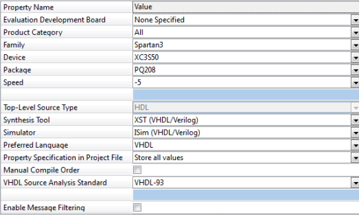
Create a new project on your P: drive. Choose a suitable name and location for the project. Make sure your Project Settings are as shown below:
From the ISE Project Navigator menu select Project > Add Copy of Source. Locate the previously downloaded files counter.vhd and tb_counter.vhd. Change the file association of ‘tb_counter.vhd’ to ‘Simulation’ (this is a testbench file, changing association ensures that it shows up in the Simulation view, but not in the Implementation view of the design hierarchy list).
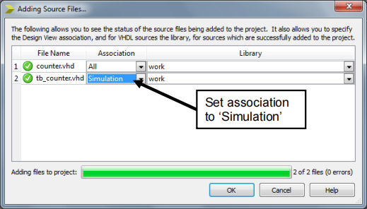
A copy of the files will be made and placed in your new project directory. Note that existing sources can be also added from the menu Project > Add Source (which does not create a copy, but just adds a file existing at some location to the project).
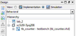
The project hierarchy list (in the Simulation view) should now show as follows:
Double-click on the tb_counter.vhd and counter.vhd to open them in the text editor. The counter module is a model of an up/down counter with asynchronous preset. Direction of counting is set by signal ‘up’, the counter should increment when up=’1’ and decrement when up=’0’ . Examine the VHDL code of the counter and the testbench, and make sure you understand it. The testbench module contains three processes. The first one generates a clock signal, the second one generates other stimuli (preset, and up signals). The third is an output monitoring process.
Simulate the testbench. Ensure the simulation runs long enough for you to view the complete waveform. You can set the simulation run time in the properties of the ‘Simulate Behavioural Model’ process, you can also change it in the ISim window that appears after a simulation is launched. Click on the “Run” ![]() button to run for a specified length of time, or you can simply use the “Run All”
button to run for a specified length of time, or you can simply use the “Run All” ![]() button on the toolbar, which will run the entire simulation – but beware, if the testbench contains looping processes and no explicit termination statements it will not end unless it is manually stopped!)
button on the toolbar, which will run the entire simulation – but beware, if the testbench contains looping processes and no explicit termination statements it will not end unless it is manually stopped!)
When simulating, it is often useful to represent binary data (bit vectors) in a more convenient format. In this case, you should tell the simulator to represent the “count[7:0]” vector as a number. To do this, right-click on “count[7:0]” in the signals list, then select “Radix” and then “Unsigned Decimal” .
TASK: Simulate the testbench and observe the waveforms to verify that the counter behaves correctly. Note that the counter does not actually count down when signal up=’0’ . Correct this error in the counter.vhd module.
After you make changes to the VHDL code, save it. You can then then reload and restart the simulation from the ISim window, by clicking on the Re-launch button: 
When designing large systems, it is often required to provide automated tests for the components. It is often impractical to require a verification engineer to actually look at the simulation waveforms to decide if the component behaves as expected. A good testbench should not only contain stimulus waveforms that thoroughly test a component, but should also contain assertions that specify what outputs are expected of a system for a given stimulus, thus providing a means of automatically testing a component.
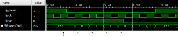
The testbench architecture in tb_counter.vhd contains a ‘monitor’ process (lines 77- 100), that contains a number of assert statements. These assertions test the value of the counter output at specific times during the simulation: 1.2 us, 2.2 us, 3.2 us, 4.2 us and 5.2 us (indicated by the arrows ↑ in the timing diagram above) so that the correct response of the component to the given stimulus can be verified. An incorrect model will produce error messages.
If the counter operation is correct the testbench terminates and reports “All tests OK. End of simulation (not a failure)”. This single message is generated by the assert statement in line 99 of the tb_counter.vhd and is used to terminate the simulation after all tests have been performed. If the simulation is not terminated in such way, it would continue forever.
Change the counter to one that increments when signal up is opposite to the original specification (i.e. increments when up = ‘0’) by replacing line 25 in the counter.vhd with:
if up = '0' then
Run the simulation, and observe the error messages in the ISim Console window.
TASK: Simulate the testbench with the modified counter component, and then again with a correct counter component. Observe the error messages. The incorrect component should terminate with an “ERROR …” message. The correct component should complete with a message: “OK. End of simulation (not a failure)” .
The assert statements must be designed together with the stimulus waveform and placed at relevant points in time during the simulation to verify whether the outputs of the unit under test are as expected. A good testbench should use carefully designed stimuli and assertions, to test every aspect of component’s functionality. The testbench you have is far from perfect, for example it does not verify whether the counter correctly counts down. Use the correct version of the counter (i.e. incrementing when up=’1’ - verify that it passes the verification test producing no ERROR messages). Then “break” the counter by replacing the line 28:
q <= q – 1;
with
q <= q;
and simulate the testbench again. The counter does not count down, but the testbench does not report any errors!
Assignment 1 - Testbench Design
A good testbench should provide a comprehensive detection of errors. On the other hand, it is extremely difficult (and most likely impossible) to test all possible cases for a more complex system, so the test strategy is always a compromise between the test coverage, and the test effort. In this exercise you should detect the following errors:
- Counting cycle not correct (should count up when up=’1’ and down when up=’0’)
- Counter triggered by the wrong clock edge (should be rising-edge triggered)
- Preset signal synchronous (should be asynchronous)
For the purpose of this exercise, you don't need to test the counter behaviour for every possible counter value and input. It is recommended that you modify the file tb_counter.vhd that you have been working on already in Exercise 1. The stimulus waveform contained there is sufficient to carryout all the required tests (to achieve full marks), but you may extend it if you wish. You need to identify at which point in time to make an assertion, and what the asserted value of the output signal should be equal to, and insert appropriate code into the output monitor process.
Your testbench will be submitted for online marking. To facilitate this, it is required that it meets the following specifications:
The testbench must be based on the tb_counter.vhd template.
The entity name must be tb_counter.
The testbench should terminate within 1 ms simulation run time.
The simulation of the correct component must terminate with an assertion of severity level FAILURE, and report string containing the word “OK”, using capital letters. For example:
assert FALSE report "OK (not a failure)" severity FAILURE;
The simulation of an incorrect component must terminate with an assertion of severity level FAILURE, and report string containing the word “ERROR”, using capital letters, and not containing the word “OK”. For example:
assert (counter = "00000000") report "ERROR – counter not zero" severity FAILURE;
You are not allowed to use packages other than std_logic_ 1164 and numeric_std.
|
Assignment 1 Submit your testbench through the DSD2 Coursework System. The testbench should identify the correctly working counter, and one which is not correct. Your testbench will be simulated, together with the correct and some incorrect components. Marks will be awarded for identification of the correct component, detection of count sequence errors, and detection of clock and reset errors. To get full marks you need to check for at least a couple cycles counting up, a couple cycles counting down, correct clock triggering edge, and the correct timing of the reset operation. |
Exercise 2. IP Cores
In this exercise, we will learn how to import an IP (intellectual property) module into a design. Many companies provide IP cores, they may range in complexity from relatively simple datapath components, e.g. a multiplier circuit, to a complex sub-system (e.g. a complete USB interface, or a PowerPC processor core). IP modules are sometimes provided as plain VHDL code, but for the reasons of IP protection, they are often obfuscated (i.e. deliberately made difficult to read and understand). Very often IP modules are provided as pre-configured logic blocks, already in a form of a netlist of a synthesised design. These netlists can take proprietary file formats (depending on the target implementation technology). They can be used (simulated and synthesised) as part of other designs, but instead of a source VHDL code, they are instantiated as “black-boxes” into VHDL designs.
In this exercise, we will use a ‘Johnson Counter’ IP core, which is provided as a pre-synthesised netlist in the .ngc file format used by Xilinx.
Download files jc.ngc and johnson.vhd. These files can be found under the Resources tab of the DSD2 Coursework System.
The file jc.ngc contains the netlist of the IP core component, and the file johnson.vhd is a VHDL wrapper, that defines the johnson VHDL entity, clearly listing its ports, and instantiates the jc black-box component as its architecture.
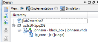
1) Create a new project. Make sure you use Spartan3, XC3S50 device in the Project Settings.
2) Add the two sources jc.ngc and johnson.vhd to the project. Your design hierarchy should look as follows:
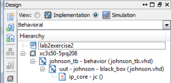
2) From menu, select Project > New Source and add a new VHDL Test Bench source. Give it a
suitable name (e.g. johnson_tb) and associate the new source with the johnson module
3) Switch to ‘Simulation’ View. Your design hierarchy should look as follows:
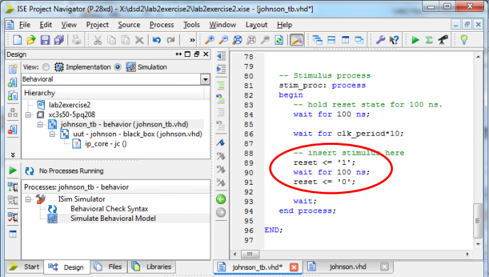
4) Edit the test bench file to add a reset pulse stimulus, as shown below:
5) Select the test bench in the design hierarchy list and launch the Simulate Behavioural Model process. Observe the simulation result. You will notice that the output of the component remains undefined!
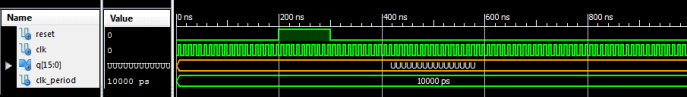
You may see warnings in the ISE Project Navigator console window, that alert you to the fact that the instance jc is an unbound black box. This is because jc is an IP core component for which you have only a pre-synthesised netlist, but no behavioural model that can be simulated! However, since the component can be synthesized, it can be then simulated based on its post-translate model.
6) Choose ‘Post-Translate’ from the pull-down list in under the Design View selection:
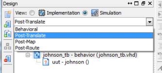
7) You can now select the test bench source and launch the ‘Simulate Post-Translate Model’ process. The entire design is first synthesized, and then simulated based on a post-translate model that is generated during the synthesis process. Observe the simulation result – it should now show a correct behaviour of a Johnson counter.

It should be noted, that the component is reset in the first 100 ns of the simulation, even though no reset signal is applied! This is because the post-translated models correspond to designs implemented on Xilinx devices, which have a power-on reset feature.
You should also observe that the outputs of the counter change with some delay after the clock edge. This corresponds to the actual delays in the implemented circuit. Measure the clock-to- output delay.
Clock to output delay in the post-translate model is equal to ...... ps.
Exercise 3. Finite State Machine
Your tasks in this exercise are to implement a VHDL module of a finite state machine (FSM), specified by a given state diagram (Assignment 2), and to develop a comprehensive testbench for this state machine (Assignment 3). Each student has a different FSM to implement. Your unique state diagram can be found in Assignment 2 section of the Laboratory 2 tab on the DSD2 Coursework System.
Assignment 2 - FSM Design
Implement the VHDL module implementing the FSM specified by your state diagram.
The FSM is synchronous, the state transitions are triggered on the rising edge of the clock signal. The state machine has five states (labelled S1, S2, S3, S4, S5). Your state machine can have a synchronous or an asynchronous active-high reset, as shown on your diagram. There is a 2-bit input i, and three one-bit outputs: x, y and z. The state diagram indicates the conditions (value of the input signal i) for state-to-state transitions. It is assumed that if a particular condition is not met, the FSM remains in the same state. NOTE: The diagrams are drawn automatically - please look carefully to identify which condition belongs to which state transition. There is always exactly one input combination per each state transition shown on the diagram.
The state diagram shows which output signals are active in which state (this is a Moore state machine). In this case, all outputs are active-high, i.e. an output name in a state bubble indicates this output is equal to ‘1’ in this state; the absence of the output name in a state bubble indicates that this output is equal to ‘0’ in this state.
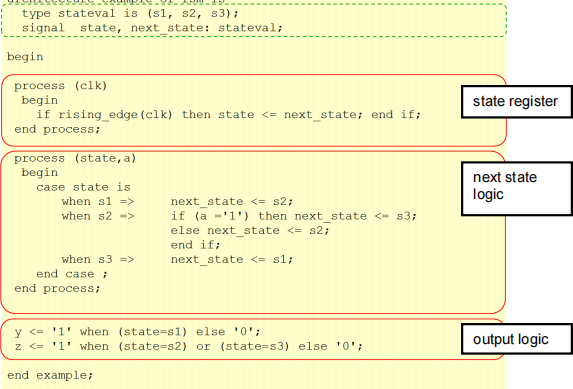
An example state machine code is provided below. This will have to be modified to fulfil your requirements! It is recommended that you clearly identify in your code the three major components of an FSM:
- sequential process representing the state register
- combinatorial section representing the next-state logic
- combinatorial section representing the output logic
You must use the following entity for your fsm:
entity fsm is
port ( clock : in STD_LOGIC;
reset : in STD_LOGIC;
i : in STD_LOGIC_VECTOR (1 downto 0);
x : out STD_LOGIC;
y : out STD_LOGIC;
z : out STD_LOGIC);
end fsm;
You are only allowed to use packages std_logic_ 1164 and numeric_std. No other package is allowed.
|
Assignment 2 Submit your FSM design through the DSD Marking System. The design must be contained in a single VHDL file, called fsm.vhd. Your FSM will be simulated, to verify its correctness. Marks will be awarded for correct implementation of state transitions, clocking and reset. |
Assignment 3 - FSM Testbench Design
Your task is to develop a VHDL testbench, capable of distinguishing between a correctly working FSM (i.e. your unique FSM, as specified by the state diagram in Assignment 2) and one that is not correct (i.e. a different FSM).
It is recommended to use the standard Xilinx testbench template, generated for the fsm component specified in Assignment 2.
The testbench entity must be called fsm_tb
Your testbench should instantiate the fsm component, as specified in Assignment 2. The testbench file should create a valid simulation when compiled together with the fsm component file. (This is ensured if the testbench is correctly associated with the ‘fsm’ module in the Project Navigator)
The testbench will be used to simulate your correct FSM, as well as a number of FSM models which do not behave in exactly the same way (having different state transitions, reset type and state, or active clock edge). A good testbench should be able to discriminate between the correct and incorrect behaviour. You should generate appropriate input signal stimuli and check the outputs to confirm the correct behaviour. You must use ‘assert’ statements, with severity level set to FAILURE, to automate the test process:
The simulation of the correct FSM must terminate with an assertion of severity level FAILURE, and report string containing the word “OK” , using capital letters. For example:
assert FALSE report "OK (not a failure)" severity FAILURE;
The simulation of an incorrect FSM must terminate with an assertion of severity level FAILURE, and report string containing the word “ERROR”, using capital letters, and not containing the work “OK”. For example:
assert (x='1') report "ERROR – output not correct" severity FAILURE;
The testbench simulation should complete within 1 ms simulation runtime (i.e. under all conditions the simulation must terminate, through an assertion of severity level FAILURE, within 1 ms) .
The testbench should start with an active reset signal to ensure the FSM is put into a known state. No assertions should be made before the FSM is reset to a known state.
The testbench should verify the behaviour of a realistic, synthesisable component description. Small variations between correct VHDL models are possible, and the testbench should not attempt to check behaviour in "unusual" cases. In particular,
- do not change any stimuli at the exact time of the active clock edge,
- do not make assertions at the exact time of the active clock edge,
- do not check for 'U' (undefined) signal values.
- do not check anything before reset (not before clock edge if the reset is synchronous!)
Please note that in the testbench you are only allowed to observe the inputs and outputs of the unit under test. The testbench cannot examine the internal signals of the fsm (in particular, the state signal is not directly accessible, and state must be inferred from the outputs)
You are not allowed to use packages other than std_logic_ 1164 and numeric_std.
Exercise 4. Mystery
For this coursework exercise each student is assigned a different ‘mystery’ FSM component. Your unique mystery FSM can be found on the Laboratory 2 - Assignment 4 tab of the on-line DSD2 Coursework System. The model is an IP core (black-box). It consists of a VHDL entity/architecture pair (mystery.vhd) and a pre-synthesised netlist (mc.ngc). The IP core can be simulated.
Assignment 4. The ‘mystery’ FSM
Download the files containing your unique mystery FSM: mystery.vhd and mc.ngc. Consult the instructions in Exercise 2 in order to create and simulate a project based on an .ngc netlist component.
Your task is to ‘reverse-engineer’ the mystery FSM, through simulations, and to create a VHDL model of this FSM.
Your VHDL model must be a straightforward, “readable” piece of VHDL code, implementing a state machine in a standard behavioural VHDL. It must provide a replacement for the mystery component, with the same functionality.
The entity must bean exact copy of the ‘mystery’ entity (the entity must be called ‘mystery’, ports have to appear in the same order as in the original). The architecture should be your own code.
The mystery FSM has 5 states, two inputs (a and b) and 3 outputs (c, d, e). It is a Moore FSM. State transitions are triggered by the rising edge of the clock signal (clk). It has an active-high reset signal (rst), which could be either synchronous or asynchronous.
You only need to replicate the function of the mystery FSM, you should not attempt to replicate the exact timing behaviour of the mystery component. The post-translate model of the mystery IP core you are simulating is the model of a physical implementation, including models of gates and flip-flops with delays. The detailed timings are not relevant in a synchronous system, as long as the clock period is large enough. In particular:
- You do not have to replicate the exact timing behaviour of the IP core. When simulating the IP core, you will notice that the output signals change a short time delay (e.g. 0.1 ns) after the clock edge (and/or asynchronous reset edge). In your model, it is allowed that they change immediately after the relevant edge event.
- The post-translate simulation of the mystery IP core includes initialisation behaviour, which provides a “power-on reset” lasting 100 ns. You do not have to replicate this behaviour. You do not have to worry about signals that are uninitialized at the start of the simulation. Instead, you should assume that there will always be an active reset signal of at least 100 ns duration, at the start of a simulation. As long as your component behaves in the same way as the mystery FSM, after such reset has been applied, the solution will be considered a correct one.
- Do not change the inputs exactly at the clock edge in your simulations. This may result in an "unpredictable" behaviour of the mystery FSM. It may behave erratically, or even enter spurious states. Inputs to a synchronous system should never change at the clock edge!
You are not allowed to use packages other than std_logic_ 1164 and numeric_std.
2023-12-11