H7068 DIGITAL SYSTEMS AND MICROPROCESSOR DESIGN: COURSEWORK 2023
Hello, dear friend, you can consult us at any time if you have any questions, add WeChat: daixieit
H7068 DIGITAL SYSTEMS AND MICROPROCESSOR DESIGN: COURSEWORK 2023
Remarks:
. All the coursework has to be done in VHDL. Coursework handed in using another language will be marked as zero.
. Coursework must be typeset.
. Never use screenshots or photograph of code in your coursework. Typeset code within your coursework report using a monospace font (e.g. courier new).
. Never use photographs of waveforms in your coursework. Use a proper screen capture tool to include a high resolution screenshot in your coursework.
. The FPGA board is not required for this coursework
. Vivado is available on all university engineering computers, accessible if you are on campus, or accessible remotely via Citrix. The free Vivavo WebPack can also be downloaded from the website of
Xilinx to run on your own computers.
a) Simulation.
Consider the register bank of the educational processor (file cpuregbank.vhd of labcpu):
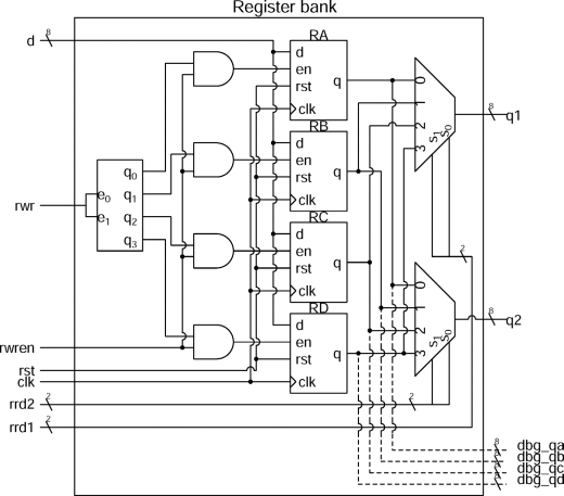
The objective is to create a testbench for this circuit, and simulate the a few operations including storing data in it as well as retrieving data from it.
In order to do this, use the file cpuregbank.vhd which is in labcpu.zip zipfile. The file dffre.vhd is also required as it is used internally by the register bank.
The ports of cpuregbank are:

The objective is to create a testbench to verify the correct behaviour of this register bank.
First, your test-bench should ensure a regular clock is driving clk with a clock period of 100ns, and a 50% duty cycle.
Then, the testbench should test a variety of operations the sequence described hereafter.
i) Reset: The test bench should first reset the register bank. The reset is synchronous. It should also set rrd1, rrd2, d, rwr, rwren to zero.
ii) Store1: store the value 0x55 to register RA
iii) Store2: store the value 0xAA to register RB
iii) Store3: store the value 0xFF to register RC
iv) Load1: get the content of register RA on q1 and RB on q2
v) Load2: get the content of register RC on q1 and RD on q2
The following points must be covered in the coursework report:
i) Explain the testbench file you constructed: what it does, and how it does it. To do this, provide the complete source of the testbench, and in the main text of your report explain the testbench file. By “explaining the testbench”, we ask you to first provide an overall explanation of how you intend to simulate the system, and then explain the purpose of each of the VHDL constructs you are using to realise the operations indicated above.
Make sure you explain where each of the operations operations (i)-(v) take place.
Note: if you create the testbench from Vivado’s user interface, a lot of default comments are inserted by Vivado. Remove these, as they are not useful for this coursework.
ii) Provide a screen capture of the waveforms resulting from the testbench. All signals must be legible. Make sure that all the values in the waveforms are legible and in hex. Note: do not take photographs! Use a proper screen capture tool, such as pressing the "Print
Screen" key. Explain what can be observed on these waveforms. Make sure you highlight on the waveform (e.g. with mspaint) where the operations Reset, Store1, Store2, Store3, Load1, Load2 operations take place.
All the register bank signals must be visible in the waveform.
[30 marks (15 marks for the testbench and associated explanation, 15 marks for the waveform and associated explanations; if the testbench does not work, not marks will be assigned)]
b) The Sussex Educational Processor executes an instruction every 3 clock cycles. Explain why that is the case and specifically what happens during each of these three clock cycles. [5 marks]
c) Explain and justify what is the maximum addressable memory for the processor using the mov instruction (note that this is not the amount of available memory, which was 32 bytes in the labs; it's the maximum amount of memory which could be ‘touched’ by the processor). [5 marks]
d) Write an assembler program which performs a multiplication of two numbers by repeated additions. The two numbers to multiply are placed in RA and RB initially, and the result after the program execution is completed must be in RC.
Note: this program must be implemented in a generic manner! If the content of the registers RA and RB were different, the program should perform the desired multiplication without any other modification than only changing the values in RA and RB in the first two instructions.
Once the multiplication is completed the program should stop (i.e. the program counter does not keep increasing to execute new instructions). You can assume that the first two lines of the program are (05h and 07h are examples of values to multiply, the program should also work with other values in the registers):
mov RA,05h
mov RB,07h
....
Address the following in the report:
i) Provide the assembler code;
ii) provide an explanation of what the assembler code does, line by line
[20 marks (10 marks for the assembler code, 10 for the explanations of the code]
e) You are provided with the following memory dump of the UoS processor code memory. Write the assembler instructions corresponding to this memory dump.
Address Data
00 1330
02 3303
04 5770
06 B10A
08 B002
[5 marks (1 per correct instruction)]
f) You are provided with the following VHDL code of a sequential element:
entity something is
port ( clk : in STD_LOGIC;
s : in STD_LOGIC;
r : in STD_LOGIC;
d : in STD_LOGIC;
q : out STD_LOGIC);
end something;
architecture Behavioral of something is
begin
process(clk)
begin
if r='1' then
q<='0';
else
if clk'event and clk='0' then
if s='1' then
q <= '1';
else
q <= not d;
end if;
end if;
end if;
end process;
end Behavioral;
The resulting circuit is a variation of a type of sequential element commonly used in digital systems.
Provide the truth table for q+.
Hint 1: there might be a “bug” or at least a subtlety in this VHDL architecture which may require you to consider rising and falling edge of signals.
Hint 2: remember how to indicate rising and falling edge in truth tables.
Hint 3: you may simulate or implement the circuit to test and verify your assumptions.
[10 marks for a correct truth table]
g) Consider the program below. Explain line by line the operation performed by the instruction and the resulting register values for registers RA, RB, RC, RD. Write the value that is in the register after the execution of the instruction in the corresponding column; if the value is
unknown indicated this with ??. Assume we do not know the content of the registers on program start.
RA RB RC RD
mov rc,92h . . . .
xor ra,ra . . . .
add ra,rc . . . .
shr rc . . . .
asr ra . . . .
[5 marks (1 mark per correct line)]
h) Explain what does the “mem addr” display show on the FPGA display, in the clock cycles fetchh, fetchl, and execute; in the case of the execute cycle, explain what mem addr shows when the instruction is a mov instruction involving memory access, and when other instructions are executed.

[5 marks]
i) Explain what issues can be encountered when using a one-hot encoding in finite state machines, and how this issue can be resolved. [5 marks]
j) Consider the instruction "MOV [RB], RD" (assume RA=08h,RB=55h,RC=37h,RD=A0h). Assume we are shortly before the clock edge of the "execute" cycle (i.e. at the next rising edge the instruction will be executed).
By analyzing the VHDL code of the processor (or simulating it!), explain what happens
inside the educational processor to execute this instruction. Specifically, indicate the state of the following signals (or indicate if undefined):
|
instruction |
(in cpu.vhd) |
|
rrd1 |
(port of cpuregbank in cpu.vhd) |
|
rrd2 |
(port of cpuregbank in cpu.vhd) |
|
rwr |
(port of cpuregbank in cpu.vhd) |
|
d |
(port of cpuregbank in cpu.vhd) |
|
reg1out |
(in cpu.vhd) |
|
reg2out |
(in cpu.vhd) |
|
source |
(in cpu.vhd) |
|
regwren |
(in cpu.vhd) |
|
flagwren |
(in cpu.vhd) |
|
ram_we |
(in cpu.vhd) |
|
ram_address |
(in cpu.vhd) |
[10 marks (proportional to the number of correct signals)]
2023-12-05