EEEE1004: INFORMATION AND SYSTEMS 2023/24
Hello, dear friend, you can consult us at any time if you have any questions, add WeChat: daixieit
EEEE1004: INFORMATION AND SYSTEMS 2023/24
Topic 1 – Digital Electronics
Coursework 1: Design and Analysis of Digital Logic Circuits
Within this coursework, you are required to work through and provide solutions to a range of problems related to Digital Electronics and Combinational Logic. There are six problems in total to complete and the marks per problem are given. Your final mark for this assignment will contribute 10% to your final grade for the Information and Systems module. The coursework assesses elements from the Digital Electronics Lectures 1-3 and Seminars 1-3 although the context of the circuit in Problem 4 is presented in Lecture 5.
You should be aware that these problems require you to take the knowledge and techniques we have studied, apply them to new scenarios and think beyond what we have covered in lectures. In addition, you will need to carefully study the ‘ Essential Information’ section below, where three additional concepts on how to represent decimal values arepresented with examples.
Instructions
You should prepare a single document with your solutions to all problems. Your work can be word- processed, handwritten and scanned, or a combination of these methods. If you are handwriting and then scanning/photographing your solutions, you must ensure that your work is legible. Within your document, number all pages and give your solutions to each problem sequentially, making sure it is clear which question (or part question) you are answering. There is no need to write out the question again in your solutions.
Ensure that you show your full working with all of your answers, including all intermediate stages (i.e., you should not just suddenly arrive at a final answer). You must submit your document before the published deadline: Tuesday 22 November 2023, 15:00 (UK time). Submission is via Moodle only – you can find the place to do this on the EEEE1004 Moodle page. Prior to submission, you must convert your work to a single PDF file (this is the only file format that will be accepted by the submission box on Moodle – it will also only accept a single file). Ensure that you click the submit button so that your work is submitted – drafts will not be marked and clicking submit after the deadline will result in a late penalty.
This coursework is an individual piece of work. Please remember your Academic Misconduct training. If you are unsure about what constitutes Academic Misconduct, please ask!
Essential Information
In the lectures, we have covered a wide range of topics involved with digital electronics and in the first lecture we met both the binary and hexadecimal (hex) number systems. These are just two common number systems, but there are several others in common usage. Over the next two pages, three new concepts on how to represent decimal values – Two’s Complement, Gray code and Binary Coded Decimal – arepresented along with details of their application and advantages.
These concepts are solely required for this coursework and so are non-examinable, i.e., the three concepts presented in this section will not feature in the final exam or any progress tests.
Two’s Complement (2’s Complement)
So far, you have been dealing with unsigned binary, where all the decimal values have been positive. However, we might also want to be able to represent negative numbers, and for this we need to use a form of signed binary. A common option here is to use a number system called Two’s Complement – often written as 2’s Complement.
In two’s complement, the most significant bit is used to indicate the sign of the value (0 representing a positive value and 1 representing a negative value) with the remaining bits used to represent the magnitude of the value. Therefore, as the MSB is solely used to indicate the sign, there is one fewer bit to represent the magnitude of the value than for a pure binary value with the same number of digits. For n-bits, the two’s complement binary-to-decimal conversion is represented as follows:
Two’s complement notation provides a convenient way of representing negative numbers and is most commonly used for integer arithmetic since it simplifies the process of binary subtraction. The notation also has a single code for representing zero (which is not the case in some other schemes not considered here).
The process to convert a negative decimal number to two’s complement binary is as follows:
1. Take the magnitude of the decimal number (i.e., take the negative number multiply it by -1).
2. Convert this positive value into pure binary (and pad with additional 0’s on the MSB side if you require a value with a specific number of bits).
3. Invert all of the bits so 1’s become 0’s and 0’s become 1’s to give a new value which is known as the one’scomplement.
4. Perform a binary addition, adding 1 to the one’s complement value.
To convert a positive decimal number to two’s complement binary, you simply convert the number into pure binary.
It is important to note that when dealing with signed binary, any padding bits on the MSB side will be 1 when the value is negative and 0 when the value is positive.
Example: Convert -210 into 4-bit two’scomplement.
Solution: Take the magnitude of -2 to give 2
Convert 2 to pure binary to give 0010 (note the additional padding 0’s here to give 4-bits) Invert 0010 to give 1101 (one’s complement)
Add 1 to 1101 to give the two’s complement value of 11102’s comp (note the inclusion of an appropriate subscript here to differentiate this from a pure binary value)
Gray Code
As with standard binary, Gray code uses n digits to produce 2n unique codes – all of which are used. The difference is that as successively higher numbers, in base-10 (decimal), are represented in Gray code, only one bit is changed at a time (this is not always the case for consecutive values when represented in pure binary – see example below).
The rule for generating Gray code is to start with all zeros which will represent decimal 0 (e.g., 0000 if we want a 4-bit Gray code), and then change the lowest significant bit that will produce a code not used before. This process of changing the lowest significant bit that will produce a further unique code is then repeated over and over. So, starting with 0000, the LSB is firstly changed to give 0001, then the second LSB to give 0011 and then it is the LSB that is changed again to give 0010, and so on. The critical point in the generation of Gray code is that only one bit changes between any pair of adjacent codes.
Gray code is of benefit when n digital signals from some kind of device, whose output consists of an n-bit binary code and where the individual bits may not always attain their correct values at the same time. For instance, consider the output of a 4-bit code indicating the state of some form of device. If the output changed from 5 to 6, then, using binary code, this would mean a change in the bit pattern from 01012 to 01102, where we can clearly see that two bits have changed their values. If the LSB changed more slowly than the second LSB, then this would lead to a transient indication of 01112 (i.e., a decimal value of 7) which may be extremely problematic. However, by using Gray code, there would be no such problem of a transient state since, by definition, there is only a 1-bit difference between any pair of adjacent codes.
Binary Coded Decimal (BCD)
One problem of binary arithmetic is that direct conversion from binary to decimal, for large numbers of many digits, requires a complex digital circuit. Therefore, often when a number is being held in a digital circuit immediately before being output to a display in decimal form, an alternative scheme known as binary coded decimal (BCD) is used rather than standard binary code.
BCD encodes each individual decimal digit with its binary equivalent, typically using 4 bits per digit unless otherwise stated.
A disadvantage of BCD is that only 10 of the possible 16 (24) unique codes that 4-bits can produce are used. Hence, it is increasingly inefficient to use BCD when representing a decreasingly large value. Nevertheless, the advantages usually outweigh this disadvantage and so it is regularly used.
Example: Convert 91610 into 4-bit binary coded decimal.
Solution: 9 in pure binary is 1001
1 in pure binary is 0001
6 in pure binary is 0110
The BCD value of 91610 is therefore 100100010110BCD (note the use of the BCD subscript here to differentiate this from a pure binary value)
Problem 1 [13 marks]
For this problem, you will work with your unique 8-digit student ID number – be sure to clearly state your ID number at the start of your solution.
a) Showing all of your working, take your 8-digit student ID and convert the value to hex.
b) How many bits would be required to represent your ID number in standard binary? Clearly
explain how you determined the number of bits (without actually doing the conversion).
c) Take your ID number and sum the individual digits together (e.g., if your ID were 30463117, the sum would be 3 + 0 + 4 + 6 + 3 + 1 + 1 + 7 = 25). State this decimal value clearly and then, showing all of your working, convert this number to both standard 8-bit binary and BCD (assuming each digit will be represented by 4 bits) .
d) Invert the decimal value that you calculated from the sum of your ID digits in Part (c) above (e.g., if the sum was 25 then your inverted value would be -25). Represent this value as an 8-bit two’s complement value, showing all of your working.
Problem 2 [10 marks]
Consider a simple line following EEEBot with four sensors, that is designed to move along a black line on awhite background as described below.
The EEEBot will move forwards only whilst ALL of the following conditions are met:
- The ultrasonic sensor (U) does not detect any obstacle
- Just the middle line following sensor (M) is over ablack line OR the middle and either the left (L) or right (R) line following sensor, are over a black line
Under any other scenario, the EEEBot stops moving.
You will design a logic circuit that processes the four inputs from the different sensors (U, L, M, R) and produces an output, F.
a) The following logic information is provided to you:
- Sensor U returns 1 if an obstacle is detected, and 0 if an obstacle is not detected.
- Sensors L, M and R return 0 if black is detected, and 1 if white is detected.
- Output F should be 1 if the EEEBot is to move, and 0 if the EEEBot is to stop moving.
Using this information, draw a truth table for this system. Take care with the definition of the logical OR operator.
b) Using a method of your choosing, obtain a Boolean expression for the output of this system. Complete any further manipulation needed to arrive at an expression from which you can draw a circuit implementation that uses the minimum number of 2-input gates (plus any NOT gates as necessary). Be sure to explain all stages of your expression and circuit development.
Problem 3 [12 marks]
A digital logic system has three inputs (X, Y, Z) and one output (Q). The completed Karnaugh map for this system is shown below.

a) Give the fundamental sum-of-products (SoP) expression for Q.
b) Using Boolean algebra, simplify the SoP expression for Q. State the law used for each step – answers that simply state the simplified expression with no intermediate steps will be awarded 0 marks.
c) Prove that your simplified answer found in Part (b) above matches the minimised expression found using a K-map approach.
d) Draw a circuit that implements your simplified expression using only 2-input AND/OR gates (plus any NOT gates as necessary).
Problem 4 [25 marks]
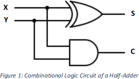
Previously, in the lecture material, you were introduced to adders, that perform the addition of two input bits (X, Y) and gives the output as two bits – asumbit (S) and a carry bit (C).
Additionally, we studied in more detail the full adder, which is a circuit that performs the addition of three input bits (X, Y, Z) and also gives the output as two bits – asum bit (S) and a carry bit (C). The circuit for a half-adder is shown below in Figure 1.
A half-subtractor and full-subtractor work in a similar way, except they perform the subtraction of two and three bits respectively, to output two bits – adifference bit (D) and a borrow bit (B).
Below in Figure 2, the circuit for a full-subtractor is shown:

a) Using the full-subtractor circuit, draw and populate the truth table for this system, using the same input and output variable names as used above.
b) From Part a), draw the K-map for each of the two outputs and find the minimised Boolean expression for each (without using the XOR operation) .
c) Redraw the half-adder circuit using only 2-input NAND gates. You must show all of your working and intermediate steps (including the truth table and K-maps) as well as ensuring that your final design uses the minimum number of gates possible.
Problem 5 [30 marks]
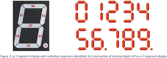
A seven-segment display, as shown in Figure 3a, consists of seven segments (S1-S7), each of which can be illuminated independently, and a decimal point (D) indicator, which can be used to indicate a number’s orientation. By controlling an appropriate combination of these segments, such a display can be used to display any single decimal digit 0-9, as shown in Figure 3b. For example, to display the decimal digit 5, segments S2, S3, S5, S6 and S7 must be lit.
You are required to design a system that will make use of this seven-segment display to act as the display to a 6-sided electronic dice. The dice will only display the decimal values of 1-6, with the digit 6 also making use of the decimal point to indicate its orientation.
Your system is to be implemented on a piece of hardware where the end user is easily able to reconfigure the logic hardware after manufacturing. Therefore, your system will also make use of Gray code to prevent spurious display outputs and the number of logic gates used is an important consideration in your design.
The system is broken down as follows:
• First, a 3-bit Binary Coded Decimal (BCD) value (A, B, C) is inputted, converted and outputted as a 3-bit Gray code equivalent value (X, Y, Z).
• Secondly, the outputted 3-bit Gray code value is inputted to another logic circuit that outputs the required eight signals (seven segments plus the decimal point) to display the correct decimal value on the seven-segment display.
For this device, each of the seven segments (S1-S7) and the decimal point (D) illuminate when supplied with a logic HIGH signal (i.e., a LOW signal to all segments would blank the display; a HIGH signal to all seven segments would display the digit 8).
a) Design the single circuit needed to convert from the 3-bit BCD input to the 3-bit Gray code output. You must show all of your working and intermediate steps as well as ensuring that your final design uses the minimum number of gates possible.
b) Determine the minimum number of gates that are required to implement the circuit that is needed to convert between the 3-bit Gray code input and the seven-segment display output, showing all of your working (i.e., truth tables and K-maps). You must clearly state how many AND, OR and NOT gates are needed (and how many inputs each gate requires) for each output (i.e., the seven segments and the decimal point). (You are only required to list the gates needed for each output - you should not draw any circuits.)
Hint: for 3 inputs there are 8 possible combinations, but as the dice is 6-sided, not all 8 of these values will occur. Ensure that you refer to Figure 3b to identify which segments need illuminating for each digit, as well as if the decimal point is needed or not in each case.
(Remember that,for this device, a HIGH signal causes illumination to occur.)
Problem 6 [10 marks]
A single 2-input XOR gate can be used to identify if two digital bits, D1 and D2, are the same or different. However, such a comparator is limited to the comparison of two individual bits. A more useful device would be one that is able to compare two N-bit digital words and report if the values of the two words are equal or if the value of one word is greater / less than the other.
Such a device can be implemented using N * 1-bit comparators, plus some other combinational logic (which is still to be designed) . Figure 4 shows a block diagram of this concept for the comparison of two 3-bit values, A = [A2, A1, A0] and B = [B2, B1, B0]. If A = B (i.e., the two 3-bit words are identical), then Output E = 1. When A > B, Output G = 1 and when A < B, Output L = 1.

In the configuration shown in Figure 4, we can just consider the 1-bit comparators as functional blocks (i.e., we know what outputs occur for different input combinations, but we are not concerned with the logic ‘inside the box’ that does it). Each single bit comparator compares bits Ai and Bi giving an output Ei = 1 if Ai = Bi, an output Gi = 1 if Ai > Bi and an output Li = 1 if Ai < Bi.
For our comparator here, the digital words,A and B, will be 3-bit two’s complement binary words.
a) State the maximum and minimum decimal values that can be compared using this 3-bit comparator (remember your 3-bit words, A and B, are in two’scomplement binary).
b) Describe in words (or you may use a flowchart if you wish) how you would compare the individual bits of A and B in order to determine whether A = B, A > B or A < B. Carefully consider the order in which you will compare the individual bits and how you will make your final decision about the magnitude of the two 3-bit two’s complement values.
c) Write Boolean expressions for each output (E, G and L) based on the Ei, Gi and Li outputs from the comparisons of the individual bits. Ensure that you clearly explain how you have developed these expressions.
2023-11-25
Digital Electronics