Lab 5: Digital System Design -Single Path RISC Architecture-Part I
Hello, dear friend, you can consult us at any time if you have any questions, add WeChat: daixieit
Digital Design and Computer Architecture
Lab 5: Digital System Design -Single Path RISC Architecture-Part I
The Goal of Lab 5 is to implement R-type instructions.
We will follow the single datapath RISC architecture (MIPS) to achieve 2 types of operations: ADD, SUB.
1. Textbook Reading
Read Slides (Lecture 9) and Reference Book (Chapter 6) on R Type instructions

and Single Cycle Microarchitecture (Lecture 10 slides and Chapter 7, see the appendix for more information).
To simplify the design, we modify the original RISC instruction op field for I-type and R-type instructions. Here, to control the 3 MUXs and ALU (RegDst, ALUSrc, ALUControl2:0, MemtoReg), we use op. The fields of op are shown below.
Note: Assume all the data in Register File is initialized as 0.
1. ADD in R-type instruction
ADD Register_File[1] and Register_File[2], and store the result to Register_File[6]. The first address rs = 1, the second address rd = 2, the destination address rt = 6; In this case, RegDst = 1, ALUSrc = 0, ALUControl[2:0] = 010, MemtoReg = 0, so:
op = 6'b100100
rs = 5'b00001
rd = 5'b00010
rt = 5'b00110
rest = 11'b0000_0000_000(shamp and funct are set as logic 0)
So, the R-type instruction should be: 32’b100100_00001_00010_00110_0000_0000_000.
2. SUB in R-type instruction
For SUB operation, it is similar to ADD in R-type instruction. Notice that ALUControl for SUB should be 110 for ALU to do subtraction.
2.Lab Tasks
1. Implement the Register File
The module of the RISC register file should look like this:
module register_file(input clk, rst,
input [4:0] A1, A2, A3, // A1, A2, A3 are the address input [31:0] WD3, //data from data memory
input WE3, //WE3 = 1, write register file
output [31:0] RD1, //output port one for register file output [31:0] RD2, //output port two for register file output [31:0] probe //probe to check the result in the
register file
);
assign probe = rf_regs[1];
// ……
endmodule
Notice for the Register File used here, we assume there are totally 32 32-bit registers, which means the width (number of bits for each register) and depth (number of registers) are both 32.
2. Initialize the Register File
Please initialize the register file as register_file[i] = i. See Appendix 1.3. on how to initialize the register file.
3. Implement ALU
The ALU header should be:
module ALU(
input [31:0] SrcA,
input [31:0] SrcB,
input [2:0] ALUControl,
output [31:0] ALUResult
);
// ……
endmodule
Note that you only need to implement ADD and SUB operations for ALU.
ALUControl = 010, do ADD, ALUControl = 110, do SUB (see Table 5.1 in Textbook)
4. Use Testbench to verify
Please use the provided testbench to verify your design. The instruction on how to use the testbench is posted on CANVAS/FILES.
The testbench is targeting the provided “top.sv” module which instantiates Register File and ALU.
5. Add a “display” module
Add a display module to the provided top module to display the result from port “probe” of Register File using 7-segment display.
3. What to Turn In?
Prelab – 2 points
- Due Date: Lab 5 pre-lab report is due in the week of 11/29.
Pre-lab report:
You must submit an electronic copy of the following items (in the correct order, and each part clearly labeled) via Canvas. All items should all be included in a single file (.pdf).
1. A screenshot of your Verilog Code for Register File.
2. A screenshot of your Verilog Code for ALU.
3. Screenshots of your output waveforms in Modelsim
(Please set your output result radix as decimal to look clearer. It’s fine if you cannot fit in all your results in one screenshot, you can separate them into several screenshots)
Notice
For simulation, we created a waveform file for testing your Lab 5 in place of the testbench, which has been added to the Lab 5 folder in Canvas/Files. For your report, you may include EITHER the results from running the testbench OR the results from running the waveform simulation. You must use one (or both, if you’d like) of these provided methods to validate your design for the pre-lab.
In-Lab – 8 points
- Due Date: Lab 5 in-lab report is due in the week of 11/29.
In-lab report:
You must submit an electronic copy of the following items (in the correct order, and each part clearly labeled) via Canvas. All items should all be included in a single file (.pdf).
1. To the pdf document from your prelab assignment, just add a section for the in-lab assignment. 2. Take 2 pictures showing your results of ADD, SUB on the 7-segment display separately.
The ADD will be adding 2 to the first digit of your board number and storing the result to register_file[1] (which the probe signal is assigned to in the example above). The SUB will subtract 3 from the first digit of your board number and store the result in register_file[1].
E.g. Your board number is 503, for ADD, you will add register_file[2] and register_file[5] and store the result which is 7 to register_file[1] and display it through a 7-segment display. Make sure you record the board number and explain which registers you use in the in-lab report.
Appendix:
1.0. Introduction - General
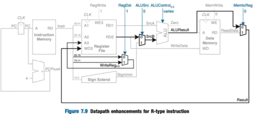
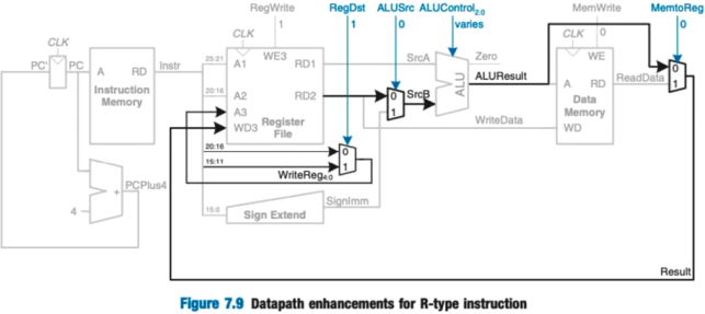
For the following labs, we are going to design a simple digital system which is a demo of a modern computer with RISC architecture. Lab 5 is part 1 of the final lab, which is to implement a single datapath RISC architecture (shown below as Figure 7.9) using Verilog.
We use the single datapath RISC architecture to achieve 2 types of operations: ADD, SUB. These 2 operations are represented into 32-bit R-type machine code in modern RISC computer architecture.
R-type Instructions
ADD and SUB are R-type Instructions. Figure 6.5 (below) is the format of an R-type instruction. All R- type instructions have a total of 32 bits.

The fields rs (instr[25:21]), rt(instr[20:16]), rd(instr[15:11]) are pointers to operands. The field op (instr[31:26]) is used for operations. In this Lab, we will not use the shamp and funct fields, so we simply set their bits as logic 0 (instr[5:0] = 6’b000000, instr[10:6] = 5’b00000).
[Important]. The values stored in rs, rt, and rd are 5-bit fields that address one of 32 registers in the register file (R).
op in R-type instructions tells us to ADD or SUB. An example will be given after we explain the single datapath RISC architecture.
1.1. Introduction - Single Datapath RISC Architecture
The main components in RISC architecture are shown below:

PC (Program Counter) contains the address of the instruction to execute.
Instruction Memory stores all the instructions. Port A requires the address of instructions. Port RD reads the instruction data. As shown here, PC connects to A and the Instruction Memory reads out the instruction from RD, labelled Instr.
Register File can read 2 registers and write 1 register simultaneously. For Register File, Port A1, A2, A3 are the input ports for address. Port RD1, RD2 are the output ports for read registers pointed to by A1 and A2, respectively. WD3 is the input port for writing data into a RF at the rising edge of the clock. WE3 is the write enable signal port.
Data Memory stores the data. Port A is the address input port. Port RD is the data output port. Port WD is the data input port. Port WE is the write enable port.
[Important] The above figure only shows the main component of a RISC architecture. A complete single
datapath RISC architecture is given in Figure 7.9. below.
1.2. Introduction - How ADD, SUB works in RISC Architecture
Please refer to Chapter 7, Single-cycle Datapath (7.3.1) in the textbook to see how ADD and SUB work in the single path RISC architecture. Here we give you a brief description on how those operations work in the RISC architecture (for details, you still need to go over the chapters/sections in textbook stated in the beginning).
Note: To better describe it, data in Register File is represented as Register_File[address]. E.g. the 1st data in Register File is Register_File[0]
ADD and SUB achieved by R-type instruction, are operations for the registers in Register File. For ADD, rs (instr[25:21]) is input to port A1 of Register File, rt(instr[20:16]) is input to port A2 of Register File. So Register_File[rs] and Register_File[rt] are read out from port RD1 and RD2 respectively to ALU to finish the addition. The ALUResult will be inputted back to Register File (Here MemtoReg = 0) from port WD3. At the same time, rd(instr[15:11]) is input to port A3 of Register File. So Register_File[rs]+Register_File[rt] is stored in Register_File[rd]. For SUB, it is very similar, please go through the textbook section 7.3.1.
1.3. An example of initializing a register file
There are a lot of ways to initialize a register file. Here we provide the simplest way to initialize it, which is to hardcode it. Below is an example of how to initialize the register file:
// suppose a register file with width=8, depth=3
reg[7:0] registers[2:0];
always@(posedgeclk or negedge reset)
begin
if(!reset) begin // active-low reset
for (int i=0; i<3; i++) begin
registers[i] <= i;
end
end
else begin
// write other logics here
end
end
Please follow the example and initialize the Register File as Register_File[i] = i.
2023-11-23
Digital Design and Computer Architecture