ELEC373 Digital Systems Design Assignment 1
Hello, dear friend, you can consult us at any time if you have any questions, add WeChat: daixieit
Department of Electrical Engineering and Electronics
ELEC373
Digital Systems Design
Assignment 1
Serial Communications
|
Module |
ELEC373 |
|
Coursework name |
Assignment 1 |
|
Component weight |
15% |
|
Semester |
1 |
|
HE Level |
6 |
|
Lab location |
PC labs 301, 304 as timetabled, at other times for private study |
|
Work |
Individually |
|
Timetabled time |
12 hours (3 hours per week – Tuesdays 1pm – 4pm) |
|
Suggested private study |
10 hours including report writing |
|
Assessment method |
Individual, formal word-processed reports (Block diagrams and ASMs can be hand drawn and scanned into the report) |
|
Submission format |
Online via CANVAS |
|
Submission deadline |
23:59 on Sunday 26th November 2023 |
|
Late submission |
Standard university penalty applies |
|
Resit opportunity |
Students Failing Assignment 1 will have Assignment 2 as the resit opportunity. Students Failing the module and Assignment 2 will have an alternative assignment in the Summer |
|
Marking policy |
Marked and moderated independently |
|
Anonymous marking |
Yes |
|
Feedback |
Via comments on CANVAS |
|
Learning outcomes |
LO1: Ability to design digital systems using the ASM design method LO2: Ability to implement digital systems using the Verilog Hardware Description Language |
ELEC 373 Verilog Assignment 1 (2023-2024)
Assignment Overview
This assignment has been set to get you familiar with designing digital systems and
synthesising them from a Verilog description. You should develop your design using Altera’s Quartus II V13.0sp1 and test your design on the Terasic DE2-35 board.
Assignment Outline
The DE2 Board has a 9 pin D type connector and associated level shifting circuitry to allow the board to be connected tothe RS232 port of another electronic device.Figure 1shows the circuit on the DE2 board which includes a MAX232 device that performs the voltage conversion and also two LEDs which indicate if there is any activity on the transmit or receive signals. These LEDs are normally off and pulse when data is being transmitted.
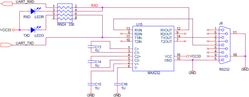
Figure 1 RS232 Level conversion circuit
Table 1shows which pins of the FPGA are connected to the MAX232 device. Note that UART_RXD is the input received signal as received on pin 3 of the 9 pin D-Type and
UART_TXD is the output transmitted signal sent to pin 2 of the 9 pin D-Type. Pin 5 carries the GND signal between the two systems.
Table 1 FPGA Pin connections

For this assignment you are to develop a UART transmitter to serially transmit data from the DE2 board, via the serial link, to a PC running a terminal program, for example “ Putty” . The PC should then display the ASCII value of the data transmitted. For example if 0x41 was
transmitted a capital ‘A’ should be displayed. The data is entered by keying in the binary
data on the “inputs” and then transmitted when the “send” key is pressed. The data should be transmitted with the baud, parity and number of bits indicated in Table 2 and also
displayed on the displays indicated in Table 2 . You should use Key[0] as a system reset, note that the Keys are active low i.e. normally high but going low when pressed.
Make sure that your design is fully synchronous,i.e. all the D type flip-flops should be clocked by the 50 MHz system clock.
Your “top level” Quartus file can be either a “bdf” or Verilog file.
Note that more modern PCs do not have a built in serial port on the Motherboard, so you
will need to use a USB to RS232 adapter cable available from the technician. To see what
communicationsport it gets mapped to, use “Device Manager” in Windows and then look at the “Ports (COM &LPT)” to see what COM port it is mapped to (it will probably be COM 4).
Reports
Your report should include the following.
1) Description of Architecture(s) and Controller(s) (with block diagram showing interconnections). (Maximum 2 pages A4)
2) Description of each module to be documented by the following information:
a. ASM Charts for any Algorithmic State Machines and any combinational logic
(Remember Combinational Logic can be treated as a single state ASM). b. Commented Verilog code for each module.
c. Full simulation of each module. (With annotations indicating what the simulation proves).
This information should be grouped together for each module i.e. there should be a single section covering the above for each module. (Don’t group all the ASMs
together, the marker needs to be able to linearly read through the report without flipping forwards and backwards. They first want to see the ASM, then the
Verilog,then the simulation for each block)
3) Schematic of the full system if a “bdf” is used otherwise the Verilog of the full system.
4) Simulation of the full system. (With annotations and maximum ½ page on any comments)
5) Explanation of experimental test results. (Max 1 page)
6) Discussion/Conclusions (Maximum ½ page)
7) You should also submit your design via CANVAS as a ZIP file. Make sure all the files need to compile simulate and test the design are included.
Please format your report in the order indicated above, i.e. fully document each module before describing the next module.
Warning
When marking the reports I will be looking very closely for any signs of collusion, as this is unacceptable. I need to assess your own ability not that of your friend or colleague. If I find any evidence of collusion then the University’s rules on the punishment for collusion will be followed. If you do collude I will spot it and you will be penalised – you have been warned.
Submission Deadline
Demonstration: Tuesday 21st November 2023
Electronic copy: Sunday 26th November 2023 @ 11:59pm on CANVAS
J.S.Smith (24/10/2023)
Notes:
1. When you have finished Assignment 1 you can start on Assignment 2 which will be to implement a full UART i.e. to add a receiver to your transmitter, which will display
the received value on some other 7 segment displays.
2. Whilst the boards have been serviced, some may still have intermittent “Keys”. It is advised to connect Key[0]-Key[3] to LEDG[0]-LEDG[3] so that you can check that
contact has been made when the switch is pressed.
3. Design using small simple modules that can be re-used, for example the same shift register design could be use in the receivers as well as the transmitter if you plan in advance.
4. Block diagrams and ASM can be hand drawn and then scanned into the report, there is no need to use a drawing package
2023-11-22
Serial Communications