ECE 310 Design of Complex Digital Systems Fall 2022 Project #1: Simple CPU
Hello, dear friend, you can consult us at any time if you have any questions, add WeChat: daixieit
ECE 310
Fall 2022
Design of Complex Digital Systems
Project #1: Simple CPU
1. Introduction
The main purpose of this project is to let you start dealing with more complex designs, and become familiar with some of the elements used within a CPU.
All code will be scanned through MOSS system ( https://theory.stanford.edu/~aiken/moss/ ) to detect plagiarism. Please feel free to discuss. But don’t look at anyone one’s code or
show your code to anyone one either. If any plagiarism is detected, strict action will be taken.
2. Learning Objectives
. Complete a design involving separate control and datapath with multiple modules
. Complete a design that includes most of the elements to be used in the CPU
3. Project Report
You are expected to turn in a report after the end of this project. Follow the project report format on the course web-site. Be sure to include all items listed in that report format for full credit.
4. Design: simplified CPU
The microcontroller designed in this assignment is a simplified version of a CPU. Specifically, four simplifications are considered as follows:
1) No off-chip memory: The instructions of the program are assumed to be in the memory. 2) The programs consist of valid instructions ONLY, i.e., you do not have to perform error
checking to detect bad instructions
3) No overflow detection is required.
4) The CPU has a synchronous reset rst. That resets all registers to zero.
5. Design: Guidelines
For the ADD, SUB, MUL, DIV and XOR operations, Modules developed in HW3, 5 and 6 need to be used. Any other implementation will be considered incomplete and only partial credits will be given which will not exceed 25% of the credit. Once the design is completed, verify that the design works as expected. A testbench and memory image file will be provided.
4. Wolfware Submission
You also need to submit your Verilog code electronically through Wolfware as proj1.v. This file should contain a module called proj1 and include the provided test bench. It may use the ‘include directive to include other files, if you wish, but they must also be submitted with Wolfware. In addition, a second program will be used to test your code that will not be provided.
Instructions set:
0x01 ADD
0x02 SUB
0x03 MUL
0x04 DIV
0x05 XOR
0x6 JUMP
0x7 JUMPZ
0x8 STORE
0x9 LOAD
They have to be implemented this way
0x01 ADD => you have to use HW3 module my8bitaddsub_gate
0x02 SUB => you have to use HW3 module my8bitaddsub_gate
0x03 MUL => you have to use HW5 module
0x04 DIV => you have to use HW6 module
0x05 XOR => you have to use 2-1 mux based XOR developed in HW3
5.1 Top-level module:
|
module proj1( clk, rst, MemRW_IO, MemAddr_IO, MemD_IO ); input clk; input rst; output MemRW_IO; output [7:0]MemAddr_IO; output [15:0]MemD_IO; |
CPU Schematic
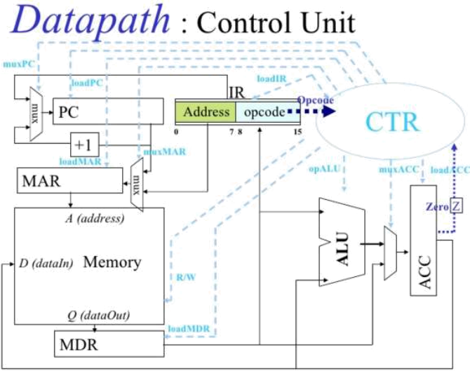
Here are the modules that needs to be coded up
All instructions are assumed to present in a memory
Module 1
The memory module:
module ram(
we,
d,
q,
addr
);
We => 1 bit read / write enable
D => 16 bit data input
Q => 16 bit data output
Addr => 8 bit input address
Module 2
Alu module
module alu(
A,
B,
opALU,
Rout
);
A => 16 bit input 1
B => 16 bit input 2
opAlu, 2 bit input, 0 = xor, 1 = a+b, 3 = negate
Rout => 16 bit output
Module 3
Controller
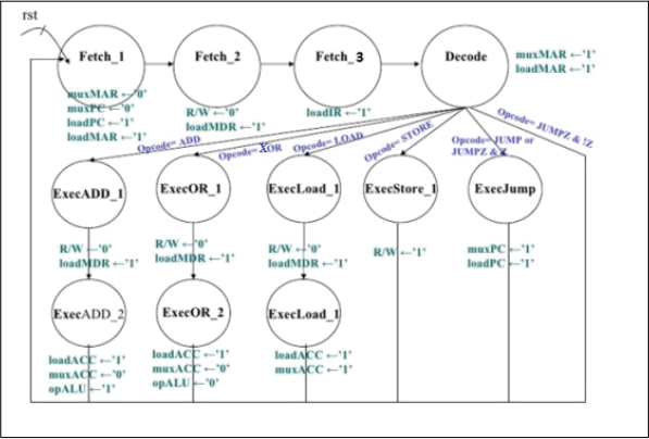
module ctr (
clk,
rst,
zflag,
opcode,
muxPC,
muxMAR,
muxACC,
loadMAR,
loadPC,
loadACC,
loadMDR,
loadIR,
opALU,
MemRW
);
input clk;
input rst;
input zflag;
input [7:0]opcode;
output reg muxPC;
output reg muxMAR;
output reg muxACC;
output reg loadMAR;
output reg loadPC;
output reg loadACC;
output reg loadMDR;
output reg loadIR;
output reg opALU;
output reg MemRW;
You will have to think about how to integrate the HW modules in to the project. A simple way would be to do DIV similar to ADD. You will have div_ 1 and div_2 to get the two parameters.
Then you will have div_3 , 4, 5 , 6 that would the 4 state machine states in HW6.
we move through the states at each clock cycle. There are only two exceptions. At decode we have to see what is the opcode and go to the next state accordingly.
At Jumpz you have to look at the zeroflag. If the flag is high, we have to execute to go to the exec jump state or go to fetch_ 1 state.
When at each of the state you will have to set all the appropriate outputs as shown in the finite state machine.
Module 4
Register bank
module registers(
clk,
rst,
PC_reg,
PC_next,
IR_reg,
IR_next,
ACC_reg,
ACC_next,
MDR_reg,
MDR_next,
MAR_reg,
MAR_next,
Zflag_reg,
zflag_next
);
input wire clk;
input wire rst;
output reg [7:0]PC_reg;
input wire [7:0]PC_next;
output reg [15:0]IR_reg;
input wire [15:0]IR_next;
output reg [15:0]ACC_reg;
input wire [15:0]ACC_next;
output reg [15:0]MDR_reg;
input wire [15:0]MDR_next;
output reg [7:0]MAR_reg;
input wire [7:0]MAR_next;
output reg Zflag_reg;
input wire zflag_next;
This is a very simple module. At reset set all registers to zero. At all other clocks cycles, All it does is at each rising edge of clock, it grabs the next value and stores it in the registers.
Module 5
Data path: In this module the next values are generated for all the registers and the singles to drive all the muxes.
module datapath(
clk,
rst,
muxPC,
muxMAR,
muxACC,
loadMAR,
loadPC,
loadACC,
loadMDR,
loadIR,
opALU,
zflag,
opcode,
MemAddr,
MemD,
MemQ
);
input clk;
input rst;
input muxPC;
input muxMAR;
input muxACC;
input loadMAR;
input loadPC;
input loadACC;
input loadMDR;
input loadIR;
input opALU;
output zflag;
output [7:0]opcode;
output [7:0]MemAddr;
output [15:0]MemD;
input [15:0]MemQ;
reg [7:0]PC_next;
wire [15:0]IR_next;
reg [15:0]ACC_next;
wire [15:0]MDR_next;
reg [7:0]MAR_next;
reg zflag_next;
wire [7:0]PC_reg;
wire [15:0]IR_reg;
wire [15:0]ACC_reg;
wire [15:0]MDR_reg;
wire [7:0]MAR_reg;
wire zflag_reg;
wire [15:0]ALU_out;
//one instance of ALU
// one instance of register.

//code to generate
[7:0]PC_next;
Only change if loadpc is enabled.
Mux pc decides between pc+1 or branch address
Reset address is 0, Hence nothing for the datapath to do at reset.
[15:0]IR_next;
Gets value of mdr_reg if loadir is set
[15:0]ACC_next;
Only change when loaddacc is enabled.
Muxacc decides between mdr_reg and alu out
[15:0]MDR_next;
Gets value from memeory, if load mdr is set
[7:0]MAR_next;
Only change if loadmar is enabled.
Mux mar decides between pcreg or IR[15:8]reg
zflag_next;
Decide based on the content of acc_reg
//needs to generate the following outputs
//set this outputs based on the registered value and not the next value to prevent glitches.
output zflag; => based on ACC reg
output [7:0]opcode; => based on IR_reg
output [7:0]MemAddr => Same as MAR_reg
output [15:0]MemD => Same as ACC reg
Module 6
High level module
module proj1(
clk,
rst,
MemRW_IO,
MemAddr_IO,
MemD_IO
);
input clk;
input rst;
output MemRW_IO;
output [7:0]MemAddr_IO;
output [15:0]MemD_IO;
//one instance of memory
//one instance of controller
//one instance of datapath1
//these are just to observe the signals.
assign MemAddr_IO = MemAddr;
assign MemD_IO = MemD;
assign MemRW_IO = MemRW;
The program to be loaded in to memory for verification
|
A test bench and a memory image memory.list will be provided. |
|
Testbench snippet always #5 clk = !clk; initial begin clk=1'b0; rst=1'b1; $readmemh("memory.list", proj1_tb.dut.ram_ins.mem256x16); #20 rst=1'b0; #40000 //might need to be very large $display("Final value\n"); $display("0x000e %d\n",proj1_tb.dut.ram_ins.mem256x16[16'h000e]); $finish; end |
2023-11-20