ELEC4602 Microelectronics Design and Technology Term 3, 2020 FINAL EXAMINATION
Hello, dear friend, you can consult us at any time if you have any questions, add WeChat: daixieit
FINAL EXAMINATION
Term 3, 2020
ELEC4602
Microelectronics Design and Technology
QUESTION 1 [25 marks]
Figure 1 shows a layout implemented in the 0.18µm CMOS process described in the information sheet. Process parameters, device equations, layer key and design rules can be found on the information sheet.

(A) Draw the x-x' cross section.
(B) Draw the circuit schematic of the layout, including transistor dimensions and types, and mark the nodes A to F on the schematic.
In the following, it is assumed that all transistors in the layout are turned on and that the voltages on nodes B, C and D satisfy VD > VB > VC.
(C) Find the capacitance between nodes B and C, CBC.
In a design, it is needed to fabricate resistors in the CMOS process described in the information sheet. Resistors can be implemented in many different ways in standard CMOS technologies, each with their own merits.
(D) Show layout drawings of two different resistor implementations and discuss their merits.
The area cost of chips manufactured with a multi-project-wafer (MPW) run is C = 1000 $/mm2 . The minimum chip area in this MPW is Amin = 4mm2 while the chip aspect ratio (length/width or width/length) must be at most 2:1. A design house wishes to use the MPW to fabricate chips containing N = 5 circuit blocks which each need P = 20 pins. Pads for pins are arranged around the chip perimeter with a pitch (pad centre-to-centre spacing) of at least L = 100µm. The layout shape of each circuit block is flexible but their area is fixed at AB = 0.5mm2 each. Layout area of pads and associated circuits can be ignored.
(E) Estimate the minimum cost of the MPW.
QUESTION 2 [25 marks]
Figure 2(a) shows a conventional 2-stage operational amplifier where cascodes (M4 and M5) have been added to the differential pair. The amplifier is implemented in the 0.18µm CMOS process described in the information sheet. Some known circuit parameters are shown in Figure 2(b). Bulk effect and, where appropriate, channel length modulation can be ignored in this question.

The compensation capacitor position achieves lead compensation in the amplifier without ex-plicitly adding a resistor. For good phase margin, the transconductances of M3 and M4 must be equal.
(A) Find the width of M4, W4.
In the following, it is assumed that the effective voltage for all NMOS devices are VEffN = 0.2V and that the bias voltages are: VB = −0.2V, VCN = 0.4V and VCP = −0.2V. (The effective voltages for the PMOS devices are of similar magnitude as VEffN). All transistors must operate in the saturation region.
(B) Find the common-mode input voltage range, of the amplifier.
In the following, it is assumed that the DC small-signal parameters for all NMOS devices (gmN and rdsN) are the same and for all PMOS devices (gmP and rdsP) are the same. The main effect of the cascodes in the circuit is to increase the output impedance of the differential pair.
(C) Find an approximate expression, given in small-signal parameters, for the amplifier DC gain, AV.
To increase the gain of the conventional two-stage operational amplifier, one could add the cas-codes to the common-source stage (M3, M9) instead of to the differential pair.
(D) Discuss the consequences of cascoding the common-source stage instead of the differential pair.
It is required that the operational amplifier bias currents are ID8 = ID9 = 32µA and that VCN = VthN+4VEff8+VSS, where VEff8 =VB−VthN−VSS. Threshold voltages and effective voltages (for a given current) varies over process corners, but may be assumed to track between transistors, and hence bias voltages should be derived from a current source. To this end, an ideal current source of magnitude IB = 16µA is available.
(E) Design a circuit that generates VB and VCN from IB.
QUESTION 3 [25 marks]
Figure 3 shows the implementation of a full-adder based on transmission gates with usual inputs A, B and CI and usual outputs S and CO. The full-adder is implemented in the 0.18µm CMOS process described in the information sheet. The full-adder operates at a supply voltage VDD = 1.8V. Simplified digital transistor models can be used in this question.
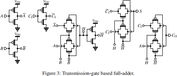
(A) Find the logic function H(A,B).
(B) Choose suitable device sizes (W and L) for all transistors, and argue for your choices.
In the following, it is assumed that all transistors have lengths L = 0.25µm and widths W = 1µm.
(C) Find the worst-case delay from A to H, t pdAH .
Full-adders are used as components in multi-bit adders. Usually this involves sections of ripple-carry connections whereby CO of each full-adder drives CI of the next full-adder.
(D) Discuss any issues you see in using the transmission-gate based full-adder in a ripple-carry adder section.
Estimation of layout area is important for good floor-planning of a chip. Layout area estima-tion can only use information available, so layout area estimation early in the design cycle can be based only on circuit schematics (including component values and dimensions) and process knowledge. It is now desired to develop a simple method to estimate the layout area of the full-adder.
(E) Argue for a suitable layout area estimation method, and estimate the layout area of the full-adder.
2023-11-20