ELEC4602 Microelectronics Design and Technology Lab 3: Op-amp design
Hello, dear friend, you can consult us at any time if you have any questions, add WeChat: daixieit
ELEC4602
Microelectronics
Design and Technology
Lab 3: Op-amp design
Objective
The objective of this laboratory session is to design and characterise a two-stage CMOS op- erational amplifier. The caracterisation is to be carried out using both hand-calculations and computer simulations. For the hand-calculations, you should use the parameters for the NCSU FreePDK 45nm CMOS process published at the course web-site. The hand-calculations should not be carried out in the laboratory session!
Op-amp design
The opamp to be designed is shown in the figure below. You should create a cell that contanins the schematic, and use suitable test-benches (as outlined in lab 2) for the different simulations that you are going to carry out. Note, that on the figure,the gate of M6 is connected to the gates of M7 and M8 – the bulk-terminal on M7 is not drawn; this is common notation for current-mirrors with multiple outputs.
Generally, it is difficult to design analogue circuits operating at supply voltage of only 0.9 V which would be required if regular transistors were used. For this reason, the opamp will be designed using the thick-oxide transistors available in the process (N THKOX and P THKOX),
 which allow for a supply voltage of 2.5 V to be used.
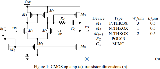
Transistor dimesions: The dimensions of most of the transistors are given in the figure; choose the dimensions for the other transistors in the op-amp.
Passive components: Passive components in your circuit must be given models suitable for
the design process used: for resistors, use the res component from the analogLib and type in POLYR in the resistor parameter field Model name; for capacitors, use the cap component from the analogLib and type in MIMC in the capacitor parameter field Model name. This is not necessary to do for components in your test benches, since the components here model loads and not explicitly instantiated components.
Parametric values: You will need to find CC and RC using simulations; to this end, it is very useful to enter their values as paramters in the schematic. Choose rc Ohms as the Resistance of RC, and cc F as the Capacitance of CC .
Building a generic testbench
Depending on the type of simulation you want to do, your test bench is going to look different. The easiest way to handle that is to build a test bench in which you can “add” or “remove” connections by entering extreme values of components (e.g. a resistor of 1 fΩ is effectivily a short-circuit, while a resistor of 1 TΩ is effectivily an open-circuit). Build the generic test bench for your op-amp shown in the figure below. v2 should be of type vpulse for transisent simulations; the other voltage sources can be of vdctype.
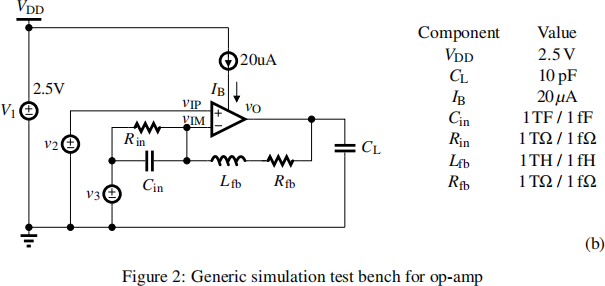
Setting design variables
Before you start the simulation, you need to choose values for the parameters cc and rc: in the
Virtuoso ADE Explorer menu, choose Variables-Copy From Cellview; that should make cc and rc appear under Design Variables in the simulation window. Now choose Variables- Edit . . . in the menu which opens a window where you can edit the design variables; set cc to 1.0pin the Value field and and set rc to 1 in the Value field; click OK. The variable values should now be set in the Setup panel of the simulation window. You should be able to do simulations now.
Finding the DC gain
To run open-loop DC simulations on your generic test bench choose the following component values:
Cin = 1fF; R in = 1fΩ; L fb = 1fH; Rfb = 1TΩ
To find the DC gain, choose v3 = vIM = 1:25V, and perform a DC analysis (as in lab 2) where
you sweep v2 around 1.25 V (you will find that the gain is very large, so in order to see a smooth
transfer function, you need to simulate in a very narrow band around the common-mode voltage
(1.25 V).) The gain is, of course, the (maximum) slope of the DC (v2 to vO) transfer characteristic.
Finding the DC offset – Monte Carlo simluations
An appropriately designed opamp has no systematic offset; i.e. when vIP = vIM , the output is very close to VDD/2 (when used on a single supply voltage); in reality, you need to apply a certain differential input voltage (the offset voltage) to make vO VDD/2. The actual offset in a fabricated circuit is then mainly due to mismatch between devices. The simulator model device mismatch using Monte-Carlo simulations: a large number of simulations (e.g. DC simulations) are carried out, each having slightly different, randomly chosen, parameters for each transistor corresponding to one particular fabricated circuit. If enough random simulations are carried out, you can get a very good idea of the range the offset voltage (or some other parameter of interest) will lie within.
To find the offset voltage range, have your DC simulation of the amplifier transfer function (i.e. the one you just found the DC gain on) set up – you will need an sweep band around the common- mode voltage of about 15mV. Then, in the in the Virtuoso ADE Explorer menu, choose Tools-Monte Carlo . . .; in the pop-up window select Run a fixed number of points, choose 50 for Number of Points, choose All for Variation (simulates both corner and mis- match variation), and tick the box for Save Waveforms (Simulation Data); click OK. Finally, in the Setup panel tick the Monte Carlo Sampling, and start the simulation with Simluation- Netlist and Run as per usual; it will take a little while for this simulation to run. Plotting vO will now get you a family of 50 transfer functions, each with a different offset.
Once you are done with the Monte-Carlo analysis, remember to un-tick Monte Carlo Sampling in the Setup panel.
Gain-bandwidth and phase margin
The value for CC = 1:0pF (cc) is not too bad; however to get a decent phase margin lead com- pensation is required, which means that you need to determine the value for RC. When doing open-loop AC simulations, it is best to provide a DC feed-back to make sure that the circuit op- erates in the high-gain region; that can also be achieved by noting the DC operating piont (as in lab 2), but that point will change, if you make a tiny change to the circuit: The following set-up is much easier. Choose the following component values:
Cin = 1TF; R in = 1TΩ; L fb = 1TH; Rfb = 1fΩ
Remember to enter both an AC Magnitude of 1 and a DC voltage of 1.25 for v2; you can now run an AC simulation; to find the unity-gain frequency plot the magnitude of output voltage (vO) in dB and find the frequency where this has reduced to 0 dB. To find the phase margin, plot the phase of the output voltage, and read this value at the unity-gain frequency.
Adding plotting expressions: to plot both phase and magnitude, it is convenient to set up ex- pressions to be plotted when simulations are run. Assuming your output node is labelled vo, in the Virtuoso ADE Explorer menu choose Outputs-Add-Expression; in the new expr line in the Output Setup, enter phase(VF("/vo")) and hit <Enter>; also add expression with dB20(VF("/vo")). Expressions can be very advanced; Cadence has an expression editor / cal- culator (for instance available via the menu as Tools-Calculator...) to assist you – feel free to explore.
Parametric sweep: to find a good value for RC, in the simulation window menu Setup panel, double-click on the rc value (1) and then on the three dots appearing next to the value – this allows you to set up a sweep for this value: in the pop-up window, first click Delete Spec; then choose From/To in the Add Specification roll-down menu; set Step Type to Decade, enter 10k in the From field, 1Meg in the To field and 2 in the Steps/Decade field.
Starting the simulations now will start a series of AC simulations with different values for RC . Choose a value for RC that give a smooth 20 dB/dec roll-off, and a good phase margin. What is your unity-gain bandwith and your phase margin?
Common-mode input range
Using AC simulations, try to change the DC value of v2 (e.g. by doing a parametric sweep) and find the allowable range for this voltage (i.e., the common-mode input range); when the voltage get too large or too small, you should see a significant deviation in the magnitude plot (e.g. significantly lower low-frequency gain).
Slew-rate
To find the amplifiers slew-rate, prepare your test-bench to do transisent simulations on a unity- gain configuredamplifier; choose the following component values:
Cin = 1 fF; R in = 1 TΩ; L fb = 1 fH; Rfb = 1 fΩ
For v2 , enter rise and fall-times of 1 ns, 50 % duty cycle, a repetition period of 3 µs, and a voltage swing between 1.0 V and 1.5 V. Now carry out a transient simulation, and note down the slew rate (i.e., the highest dvO /dt) for both for rising and falling edges. Why are they different?
Report
A short report in .pdf format on the laboratory exercise must be prepared and uploaded on the course Moodle site no later than the due date. This need to include:
. Your schematic of the op-amp gate.
– Include brief explanation of chosen transistor sizes.
. Your schematic of the test bench.
. Your DC simulation.
– On which you read the DC gain (compare this with simple hand calculations).
. Your Monte-Carlo simulation.
– On which you read worst-casre DC offset.
. Your AC simulations for different RCs.
– On which you read unity-gain frequency and phase margin (compare the unity-gain frequency with simple hand calculations).
. Your AC simluations for finding the common-mode range.
– On which you read the common-mode range (compare this with simple hand calcu- lations)
. Your Transient simulations.
– On which you read the slew rates (compare this with simple hand calculations)
2023-10-23