CSSE4010 – Digital System Design Prac 4
Hello, dear friend, you can consult us at any time if you have any questions, add WeChat: daixieit
CSSE4010 – Digital System Design
Prac 4 - Finite State Machine
NOTE: Things can take time. So be prepared with the lab activity, do all the preliminary designs and as much implementation as you can beforehand.
Design Task
Design a sequence detector that raises an output Z a flag for two clock periods when the input sequence is 11001. The detector must continue checking the serial input while the flag Z is raised (detect overlapping sequences, such as …110011001… and raise the flag twice in this case). Each time the flag is raised it should retain at high for two clock periods. Design the sequence detector as synchronous FSM(s).
There might be several approaches to achieve the above functionality. Draw state diagrams and discuss your solutions with a tutor before attempting to code in VHDL. You must have an optimised state diagram before start implementing. State any assumptions you make.
Approach 1 – use a single FSM. This is the most primitive approach and you might see that if one wants to keep the flag raised for more clock periods and also if the overlap length of the sequence increases, the additional states required in this approach will grow exponentially and thus, doesn’t scale well.
Approach 2 – using interacting FSMs (covered in the tutorial of week 6). Whenever there are separate sequential tasks, such as detecting the sequence and keeping the flag high for 2 clock periods in this case, you could have two FSMs operating in parallel, driven by the same clock (i.e. synchronous). Use FSM1 for detecting the sequence, FSM2 for rising and holding the flag. You will need to generate a signal from FSM1 to start FSM2 early enough to make them interactive. Also think about the most appropriate model (Meely or Moore) for FSM1 and FSM2. Get your paper design verified by a tutor.
You should present and analyse both approaches in your report in terms of state diagrams. However, you are only required to implement and test approach 2 in VHDL.
1. Implement approach 2 above in VHDL using two interacting FSMs. You can use any abstraction level as you wish. You can either let the tool to do state assignments or you could make your own state assignments based on the heuristic rules mentioned in the lectures. The inputs to your top-level entity should be:
• Clock – the clock signal
• Input – the serial bit pattern in
• F – the sequence detection output flag
• Reset – asynchronous reset input (should be active low)
2. Simulate your design and test exhaustively for correct functionality. Make sure all state transitions are operational. Your testbench should generate the clock and the input test sequence and you should demonstrate at least one non-overlapping detection and one overlapping detection in your output.
3. Testing with the FPGA board is optional for this lab.
A typeset PDF report must be submitted by the due date with the following content:
Introduction stating the problem description, any assumptions, and design objectives
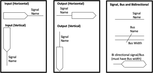
Design description including a block diagram explaining the complete design. Block diagrams should be drawn using standard symbols for inputs/outputs, signals and busses as shown below.
• Description of the two design approaches including state diagrams. Properly indicate all the
state transitions, outputs and state names.
• Detailed simulation results showing the key scenarios to prove that the design is functionally correct and delivers the expected output. At least one overlapping and one non-overlapping detection of the given sequence.
• Register transfer level (RTL) schematic of the design obtained from Vivado tools (you should try to back-annotate the RTL schematic and try to identify the basic sub-systems/blocks in your design)
• Synthesis schematic and results including FPGA resource consumption
• Conclusion – a reflection of what you’ve achieved in this exercise, problems (if you had any) and potential improvements to your design (if any)
• References (if any)
• You must have the marking sheet on the next page as the last page of your report and your marks will be indicated on this sheet (this has also been uploaded on BB as a single pdf file so that you can append this to your report as the last page)
The pracs in this course are marked to a specific criteria. This means you must demonstrate sufficient understanding and functionality and the marking will be done according to the rubric provided below. You must attempt each prac (i.e., a report must be received by the due date) to pass the course. All designs VHDL code used must be your own work. You are NOT permitted to use other VHDL code sources, unless directed to. Plagiarism is unacceptable and please read and understand the School Statement on Misconduct, available on the ITEE website at:http://www.itee.uq.edu.au/itee-student-misconduct-including-plagiarism . To avoid problems make sure that your VHDL code is the product of your work and do not let anybody else 'reuse'your code.
|
Marks |
Criteria |
|
Simulation |
|
|
0 |
Simulation not attempted or does not work |
|
1 |
Simulation works only for non-overlapping sequence detection |
|
2 |
Simulation works only for overlapping sequence detection |
|
3 |
Simulation fully works for both overlapping and non-overlapping cases |
|
4 |
Simulation fully works for both overlapping and non-overlapping cases with output retained for two clock periods |
|
Report |
|
|
0 |
No evidence of content or work |
|
1 |
Some content, insufficient explanation of circuit |
|
2 |
Reasonable content, some explanation of circuit (both approaches are explained) |
|
3 |
Good content, reasonable explanation of circuit (both approaches are explained) |
|
4 |
Excellent content, good explanation of circuit (both approaches are explained) |
|
Oral assessment |
|
|
0 |
No knowledge of the design (total mark will be capped at 0%) |
|
1 |
Very little knowledge of the design (total mark will be capped at 50%) |
|
2 |
Reasonable knowledge of the design |
|
3 |
Good knowledge of the design. |
|
4 |
Excellent knowledge of the design. |
|
Total (12): |
Marker Initials:
Date: |
2023-09-13
Finite State Machine