ELEC 271 ELECTRONIC CIRCUITS AND SYSTEMS Second Semester Examinations 2015-16
Hello, dear friend, you can consult us at any time if you have any questions, add WeChat: daixieit
ELEC 271
Second Semester Examinations 2015-16
ELECTRONIC CIRCUITS AND SYSTEMS
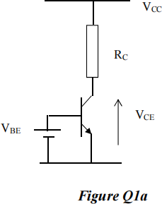
1 a) Consider the circuit of Fig Q1a). The transistor can be considered to be ideal and VBE is a fixed value of about 0.6 V. (Assume the transistor always operates in the active regime.)
i) If the resistor RC is doubled in value, do you expect IC to increase, decrease or stay the same?
ii) What would happen to IC ifVCC is doubled?
Briefly explain the reasons for your answers.
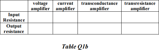
b) Copy table Q1b) into your answer book. Complete the table with the words ‘infinite’ or ‘zero’, to specify the values of input and output resistances for the four generic types of amplifier. All amplifiers can be considered ideal.
![]() c) Figure Q1c) shows an amplifier system. The source has low internal impedance and the load has a small resistance. Choose a suitable generic amplifier type to ensure good matching between source and load. Hence sketch a systems diagram with appropriate equivalent circuits for the source (Thevenin or Norton) and generic amplifier type.
c) Figure Q1c) shows an amplifier system. The source has low internal impedance and the load has a small resistance. Choose a suitable generic amplifier type to ensure good matching between source and load. Hence sketch a systems diagram with appropriate equivalent circuits for the source (Thevenin or Norton) and generic amplifier type.

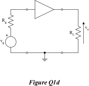
![]() d) An ideal transconductance amplifier is connected as shown in Fig. Q1d). The overall voltage gain of the circuit, vo/vg is 300 when RL is 10 kΩ. Calculate the gain of the ideal transconductance amplifier.
d) An ideal transconductance amplifier is connected as shown in Fig. Q1d). The overall voltage gain of the circuit, vo/vg is 300 when RL is 10 kΩ. Calculate the gain of the ideal transconductance amplifier.
![]() e) Use the given equation for the drain current of the MOSFET in saturation to show that the transconductance, gm and output conductance, gds of the MOSFET are given by the following expressions:
e) Use the given equation for the drain current of the MOSFET in saturation to show that the transconductance, gm and output conductance, gds of the MOSFET are given by the following expressions:

f) What is the function of the section of circuit shown in Figure Q1f).
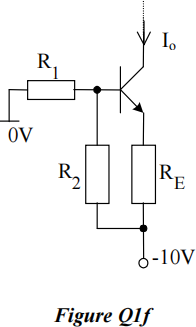
Calculate the value of Io ifR2 = 4R1 and RE = 7.3 kΩ .
g) An operation amplifier with a slew-rate limit of 1V/µs is required to amplify a sinusoidal 100 kHz signal. Calculate the maximum amplitude of the output voltage that can be achieved without distortion.
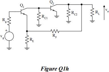
![]() h) Figure Q1.h) shows a schematic diagram of a feedback amplifier with bias components and coupling capacitors removed. Identify the feedback topology and the amplifier type. Hence write down an expression for the feedback fraction, β .
h) Figure Q1.h) shows a schematic diagram of a feedback amplifier with bias components and coupling capacitors removed. Identify the feedback topology and the amplifier type. Hence write down an expression for the feedback fraction, β .
Total 40
2. a) You are required to design a 2-stage voltage amplifier (find values for RE, RC1, RC2) to meet the following criteria: an input resistance of 400 kΩ and an overall voltage gain equal to or greater than 250, with a resistor output load, RL. Use a common-emitter with emitter degradation (RE) stage for the input, followed by a common-emitter amplifier with bias current equal to 0.5 mA.
(VCC = 20 V, βo = 200 and the DC levels of the first and second stage outputs need to be set at half the supply voltage. Allow 10% of VCC across RE). Proceed as follows:
i) Draw a schematic circuit of your amplifier, omitting the bias resistors and coupling caacitors.
ii) Work out the bias current and emitter resistor value to meet the input resistance specification. Hence find the value of the collector resistor of the first stage.
iii) Work out the gain of the first stage and hence find the required gain of the 2nd stage to meet the specification.
iv) Estimate the minimum value of load resistance, RL to satisfy the specification of voltage gain.
b) Comment on the ‘quality’ of your voltage amplifier and suggest how it could be improved.
Total 20
3. Figure Q3 shows an amplifier where the bias resistors and coupling capacitors are omitted for simplicity.
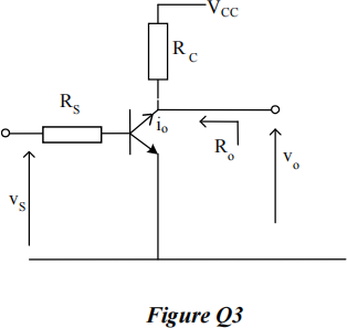
The amplifier operates with a bias current of IC = 1 mA and you may assume that rbb’ = 0 Ω. Other parameters are βo = 100, RC = 2.5 kΩ, Cbc = 1 pF, RS = 1 kΩ and  with fT = 200 MHz,. (recall that g = 40 × IC ).
![]() a) Draw the ac equivalent circuit of the amplifier at high frequency. Apply Miller’s theorem, and hence represent the circuit as two independent first order circuits. Estimate values for the input and output time constants (recall that gm × rbe = βo ).
a) Draw the ac equivalent circuit of the amplifier at high frequency. Apply Miller’s theorem, and hence represent the circuit as two independent first order circuits. Estimate values for the input and output time constants (recall that gm × rbe = βo ).
b) Hence show that the voltage gain can be given by:

where the bandwidth,fH is given by  with R = rbe //RS and
C ≈ Cbe + g![]() m RC
m RC ![]() Cbc
Cbc
Calculate a value for the bandwidth.
[Ensure that you show all necessary circuit diagrams in your solutions]
c) The transistor is now loaded with a capacitor of value 1 nF (attached across the output terminal and ground). Estimate the new time constant for the output side of the circuit and hence the bandwidth. Comment on the result.
Total 20
4 a) Draw the block diagram of a simple negative feedback system. Define the terms: open loop gain, Aoℓ , feedback fraction, β and closed loop gain, Af. Hence derive the expression for the closed loop gain:

b) An amplifier with an open loop gain of 500 operates in an environment where a certain temperature rise causes the open loop gain to increase to 550.
Treating the amplifier as a negative feedback system, find the necessary feedback fraction, β to ensure that that the closed loop gain does not change by more than 0.2%. Assume that β does not change with temperature.
Hence find the closed loop gain of the amplifier to satisfy this condition.
c) A practical circuit to implement the amplifier is shown in Figure Q4c overleaf.
Show that the voltage gain is given as

and hence design the amplifier (choose suitable resistor values) to achieve the requirement found in part b). Justify any approximations used.
[If you were unable to complete part b), assume Af = 11]
.

Total 20
2023-09-03