ELEC 212 CMOS INTEGRATED CIRCUITS SECOND SEMESTER EXAMINATIONS 2018/19
Hello, dear friend, you can consult us at any time if you have any questions, add WeChat: daixieit
ELEC 212
SECOND SEMESTER EXAMINATIONS 2018/19
CMOS INTEGRATED CIRCUITS
1. a) Describe in short statements the meaning of ‘conduction band’, ‘valence band’, and ‘bandgap’ in semiconductors.
b) Draw the energy band diagram of a semiconductor and an insulator and label each part of the diagram. Explain their main difference using these diagrams.
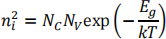
c) i) The intrinsic carrier concentration in semiconductors is described by the equation below. Explain each term.
ii) A semiconductor has intrinsic carrier concentration of 2 × 10¹⁹ m-3, NC = 1 × 1025 m-3, and NV = 6 × 1024 m-3 . Calculate the band gap of this semiconductor in eV at room temperature.
d) You are asked to design the doping process of lightly doped p-type (p-) Si wafers with resistivity of 1.5 Ω m. Mobility of holes is 0.045 m2/Vs.
i) Calculate the concentration of dopant atoms to achieve the above resistivity.
ii) State one possible dopant for this process.
iii) Calculate the position of the Fermi level in eV from the valence band edge of this semiconductor.
e) Describe with the help of a diagram the one sided pn junction and explain its main differences with a two sided junction.
f) You are asked to design a one sided Si p-n+ junction with ideal reverse saturation current of 100 pA (1 pA = 1 × 10-12 A) at room temperature (300 K). The depletion width in the n+ side is assumed negligible. The reverse saturation current of a one sided junction is described by

i) Describe each term in this equation.
ii) Calculate the doping concentration in the p-type Si to achieve the required reverse saturation current of 100 pA, where
A = 1 × 10⁻⁴ m2, Dn = 0.002 m2/s, and Ln = 1 μm (1 × 10⁻⁶ m).
iii) You are asked to reduce Is from 100 pA to 10 pA. The doping concentration cannot be changed. Explain what other device parameter can be changed to reduce Is and calculate the new value for that parameter to achieve Is = 10 pA.
Total 40
![]() 2. a) Draw the energy band diagram for an ideal MOS capacitor with p-type substrate in inversion. Show the Fermi levels, intrinsic level and band edges. On the diagram, indicate the surface potential, and the position of inversion and depletion layers.
2. a) Draw the energy band diagram for an ideal MOS capacitor with p-type substrate in inversion. Show the Fermi levels, intrinsic level and band edges. On the diagram, indicate the surface potential, and the position of inversion and depletion layers.
b) Derive an equation for the threshold voltage of an ideal MOS capacitor with p-type substrate in terms of the thickness of the oxide (tox), the permittivity of the gate dielectric (Eox) and the substrate (Es), the substrate doping concentration (NA), and the Fermi potential ψB

c) You are asked to design a MOS capacitor as described in 2b) to have a threshold voltage of VT = 1.2 V.
i) What is the gate oxide thickness for the MOS capacitor that would provide the required threshold voltage? Assume the p-type substrate doping is 2 × 1016 cm-3 .
ii) The doping concentration is increased by 10 times. Calculate and comment on the gate oxide thickness to keep the same threshold voltage.
d) Draw the capacitance voltage (CV) plots of an ideal MOS capacitor with p-type substrate at high frequency (1 MHz) and at very low frequency (10 Hz or quasi static). On the plots, label the accumulation, depletion, and inversion regions, and flat band capacitance. Explain why the capacitance in the inversion region is different when is measured at high and very low frequencies.
Total 30
3. a) Draw the cross-section of an n-channel MOSFET and label all regions.
b) i) State the difference between enhancement and depletion type MOSFETs.
ii) Draw the symbols and transfer characteristics of n-channel and p-channel MOSFETs of the two types described in i).
c) Explain the operation of a CMOS inverter. Explain its advantages and disadvantages compared to nMOS inverters.
d) Explain the issues related to the use of NOR versus NAND gates in CMOS integrated circuit design.
e) You are asked to design a two input NAND gate for a process technology with the gate length of L = 0.5 µm. The aspect ratio of a minimum size symmetric inverter is W/L = 2. What are the required aspect ratios ( W/L) of nMOS and pMOS transistors in this design?
Total 30
2023-09-03