ELEC 212 CMOS INTEGRATED CIRCUITS SECOND SEMESTER EXAMINATION 2019/20
Hello, dear friend, you can consult us at any time if you have any questions, add WeChat: daixieit
ELEC 212
SECOND SEMESTER EXAMINATION REPLACEMENT 2019/20
CMOS INTEGRATED CIRCUITS
1. a) The De Broglie hypothesis implies the wave-particle duality for an electron.
State this relation and explain the significance of each term.
b) Derive and illustrate with the aid of a diagram, the kinetic energy versus wave vector for a free electron. Explain terms ‘wave vector ’ and ‘free electron ’.
c) Explain the formation of an energy gap by considering the potential and kinetic energy of electrons in a semiconductor lattice.
(Limit your answer to 200 words.)
|
d) |
The doping concentrations of p- and n-type silicon are 5´ 1017 cm-3 and 1´ 1016 cm-3 respectively. Assume a temperature of 300 K. i) Calculate values of the Fermi potential for p- and n-type silicon. ii) Calculate the built-in potential for a pn-junction fabricated from these p- and n-type semiconductors. iii) Calculate the depletion width for the pn-junction in ii). iv) If the pn-junction is to be designed so that its depletion width is mainly on the p-type side of the junction, comment on how the doping concentrations above need to be changed. Draw the cross-section of the junction in this case and label its depletion width. |
e) Draw an energy band diagram for the pn junction in d) under the zero bias condition. Label the band edges, the extrinsic and intrinsic Fermi levels. Explain the meaning of the terms: ‘band edges’, ‘extrinsic Fermi level’,
‘intrinsic Fermi level’, ‘Fermi potential’ and ‘built-in voltage’ .
Total 40
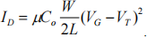
2. a) Explain what is meant by the term ‘gradual channel’ and hence derive an expression for the current flowing down the channel of an n-MOSFET in terms of the gate (VG) and threshold (VT) voltages, in the saturation region (above pinch off):
(The full mark depends on the details of your answer and how well you have explained the derivation of the equation above.)
b) Define the device constant in the equation in (a). What parameters can the designer vary and why?
c) Explain the meaning of the ‘pinch-off’ condition with the aid of a labelled cross-section of an n-MOSFET showing the channel and other regions.
d) You are asked to design a symmetric complementary metal oxide semiconductor (CMOS) inverter.
Assume the mobilities of electrons and holes are µn = 545 cm2 / Vs and µp = 130 cm2 / Vs respectively, the threshold voltages for p- and
n-MOSFETs equal to VTn = |VTp | = 0.7 V, VDD = 5 V, and aspect ratio for p-MOSFET (W/L)p = 8.
i) What is the minimum aspect ratio (W/L)n for an n-MOSFET which would meet this requirement? (State clearly all your working.)
ii) Is the CMOS inverter a ratioless or ratioed logic circuit? Explain your reasoning with the aid of diagrams.
Total 30
3. a) Draw a plan view (layout) of a CMOS inverter including polysilicon and aluminium lines, contacts and implants.
b) State the two key parameters, which govern the speed of CMOS inverters and their significance in scaling CMOS to smaller dimensions.
c) A two-input NOR gate is to be made in CMOS technology. Draw the circuit diagram and describe the principles involved in its design.
d) Design the aspect ratio (W/L)p for p-MOSFETs for the circuit in c) so that the CMOS NOR gate has symmetric transfer characteristic.
Assume VDD = 3 V, threshold voltages of n- and p-MOSFETs equal, with
VTn = VTp = 0.3V, (W/L)n = 2 for n-MOSFETs, and ratio of electron and hole mobilities µn / µn = 2.5.
Show clearly all your working.
e) Sketch two single-input domino CMOS logic gates connected in cascade.
Draw the voltage waveforms during the evaluation phase. Explain the circuit operation.
(Limit your answer to 200 words.)
Total 30
2023-09-01