ELEC 271 ELECTRONIC CIRCUITS AND SYSTEMS Second Semester Examinations 2016-17
Hello, dear friend, you can consult us at any time if you have any questions, add WeChat: daixieit
ELEC 271
Second Semester Examinations 2016- 17
ELECTRONIC CIRCUITS AND SYSTEMS
1. a) Explain what is meant by the term ‘small signal equivalent circuit’. How is it used in electronics design?
![]() b) Figure Q1b shows a transistor amplifier circuit in which the quiescent DC collector current is 1 mA. Assuming that rce maybe neglected, calculate the voltage gain vo/vi. What is the application for this circuit?
b) Figure Q1b shows a transistor amplifier circuit in which the quiescent DC collector current is 1 mA. Assuming that rce maybe neglected, calculate the voltage gain vo/vi. What is the application for this circuit?

![]() c) Consider a MOSFET common-source amplifier where the bias resistors can be ignored. Draw the ac equivalent circuit of the MOSFET device with zero load resistor and hence show that the gain-bandwidth product is given approximately by,
c) Consider a MOSFET common-source amplifier where the bias resistors can be ignored. Draw the ac equivalent circuit of the MOSFET device with zero load resistor and hence show that the gain-bandwidth product is given approximately by,

Where gm is the transconductance and C is the sum of gate-source and gate-drain capacitance. State any approximations employed.
d) Explain physically, the Miller Effect. How does it influence the amplifier performance? Suggest a circuit configuration that does not suffer from Miller Effect and explain why.
e) The triangular element in the circuit shown in figure Q1e) represents an ideal current amplifier with a gain of 50. Workout the value of the voltage gain if Rg = 5 kΩ and RL = 10 kΩ.

f) Draw an appropriate equivalent circuit for the amplifier shown in Figure Q1f, and hence derive the following expression for the loop gain:

The parameter rd is the amplifier input resistance, ro its output resistance and Aol is its open-loop gain.
![]() g) Figure Q1g shows an inverting operational amplifier circuit. Identify the feedback topology used in the circuit. Describe briefly the effect that the feedback will have on the input resistance Ri and output resistance Ro of the circuit.
g) Figure Q1g shows an inverting operational amplifier circuit. Identify the feedback topology used in the circuit. Describe briefly the effect that the feedback will have on the input resistance Ri and output resistance Ro of the circuit.

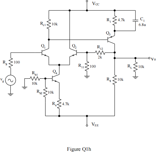
![]() h) Referring to Figure Q1h, estimate the voltage at the collector of transistor Q1 and hence the collector current of transistor Q3. What is the function of the circuit block represented by transistors Q1 and Q2?
h) Referring to Figure Q1h, estimate the voltage at the collector of transistor Q1 and hence the collector current of transistor Q3. What is the function of the circuit block represented by transistors Q1 and Q2?
What types of output sensing and input summing are being used in this amplifier?
VCC = 10 V, VEE = -10 V and DC current gain, βis large for all transistors.
2 Figure Q2 shows a two-stage voltage amplifier with bias components, coupling and DC blocking capacitors omitted for clarity.

You are required to design the amplifier to achieve an input resistance, Ri = 100 kΩ and an overall voltage gain equal to or greater than 200, into a resistor output load,
RL. The common-emitter stage (T2) has bias current equal to 0.5 mA.
VCC = 20 V, βo = 200, RS = 20 kΩ and the DC levels of the first and second stage outputs need to be set at half the supply voltage. Allow 10% of VCC across RE.
Proceed as follows:
![]() a) i) Use the chain rule to show that the system voltage gain is given as:
a) i) Use the chain rule to show that the system voltage gain is given as:
![]() ii) Workout the bias current (IC1) and emitter resistor value to meet the input
ii) Workout the bias current (IC1) and emitter resistor value to meet the input
specification. Hence find the value of the collector resistor of the first stage.
![]() iii) Workout the gain of the first stage and hence find the required gain of the
iii) Workout the gain of the first stage and hence find the required gain of the
![]() 2nd stage to meet the specification. Find also a value for RC2 .
2nd stage to meet the specification. Find also a value for RC2 .
iv) Find a minimum value of the load to achieve the required gain.
![]() b) Comment on the ‘quality’ of your voltage amplifier and suggest how it could be improved.
b) Comment on the ‘quality’ of your voltage amplifier and suggest how it could be improved.
![]() Total 20
Total 20
![]() 3 a) Figure Q3 shows the circuit of a basic operational amplifier made up of individual stages that have been identified as 1 to 5. Briefly describe the purpose of each of these stages.
3 a) Figure Q3 shows the circuit of a basic operational amplifier made up of individual stages that have been identified as 1 to 5. Briefly describe the purpose of each of these stages.
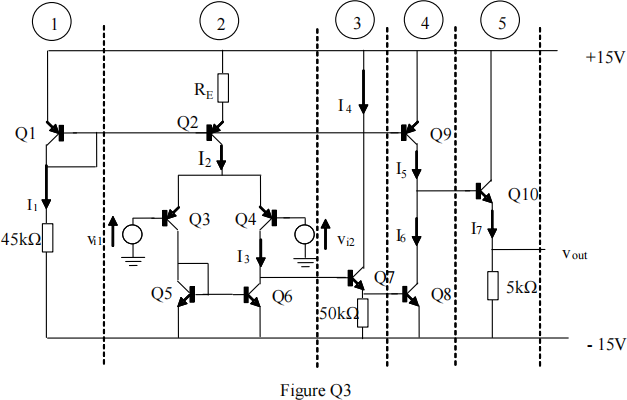
![]() b) If I2 = 0.2 mA, make reasonable approximations to estimate the total DC current drawn by the circuit from the ±15V DC voltage supply when the amplifier is biased so that the DC value of Vout = 0 V and the ac input signals are zero.
b) If I2 = 0.2 mA, make reasonable approximations to estimate the total DC current drawn by the circuit from the ±15V DC voltage supply when the amplifier is biased so that the DC value of Vout = 0 V and the ac input signals are zero.
c) Assuming that the voltage gains of the two common collector stages 3 and 5 are both unity, make reasonable approximations to estimate the overall small signal voltage gain of the amplifier, AV, where:

Assume that all the transistors have an ac current gain, βo = 100 and large DC current
gain. The Early voltage, VA = 100 V and transistor output resistance can betaken as
 where IC is the bias current. You should use the attached equation sheet.
Total 20
4 a) List the advantages and disadvantages of using negative feedback in electronic systems.
b) Draw a block diagram of an amplifier with feedback, labelling clearly the open loop gain Aol and feedback fraction, β. Show that the gain with feedback is given by

Under what conditions is the closed loop gain insensitive to variations in the open loop gain?
c) Identify the feedback topology of the amplifier shown in Figure Q6c and hence the amplifier type. Represent the circuit as a negative feedback system and hence estimate the appropriate gain.
State approximations used in your analysis.
Total 20

2023-08-29