ELEC 271 ELECTRONIC CIRCUITS AND SYSTEMS SECOND SEMESTER EXAMINATIONS 2018/19
Hello, dear friend, you can consult us at any time if you have any questions, add WeChat: daixieit
ELEC 271
SECOND SEMESTER EXAMINATIONS 2018/19
ELECTRONIC CIRCUITS AND SYSTEMS
![]() 1. a) Consider the circuit of Figure Q1a. The transistor can be considered to be ideal, it is operating in the active regime and VBE is a fixed value of about 0.6 V. If the resistor RC is doubled in value, do you expect IC to increase, decrease or stay the same? What would happen to IC if VCC is doubled? Explain the reasons for your answers.
1. a) Consider the circuit of Figure Q1a. The transistor can be considered to be ideal, it is operating in the active regime and VBE is a fixed value of about 0.6 V. If the resistor RC is doubled in value, do you expect IC to increase, decrease or stay the same? What would happen to IC if VCC is doubled? Explain the reasons for your answers.

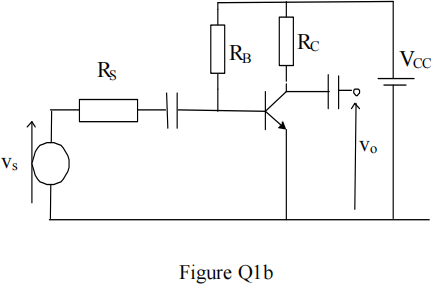
![]() b) Figure Q1b shows a common-emitter amplifier circuit. Sketch the small signal equivalent circuit for the amplifier and show that the theoretical maximum possible voltage gain is given by 40VCC. Comment on the ideal values required for RS and RB for the maximum gain condition.
b) Figure Q1b shows a common-emitter amplifier circuit. Sketch the small signal equivalent circuit for the amplifier and show that the theoretical maximum possible voltage gain is given by 40VCC. Comment on the ideal values required for RS and RB for the maximum gain condition.
![]() c) Figure Q1c shows a common emitter amplifier with emitter degradation. Calculate the dc collector current required to produce an ac input resistance of 100 kΩ, Take RE = 100 Ω and the ac current gain of the transistor as βo = 150.
c) Figure Q1c shows a common emitter amplifier with emitter degradation. Calculate the dc collector current required to produce an ac input resistance of 100 kΩ, Take RE = 100 Ω and the ac current gain of the transistor as βo = 150.

![]() d) For the level shifter circuit of Figure Q1d, work out a value for the voltage difference (V1 – V2). The transistors are identical, dc current gains are large and VBE = 0.6 V.
d) For the level shifter circuit of Figure Q1d, work out a value for the voltage difference (V1 – V2). The transistors are identical, dc current gains are large and VBE = 0.6 V.

e) Copy the table shown in Figure Q1e into your answer script and complete it with the words ‘infinite’ or ‘zero’, to specify the values of input and output resistance for the four generic types of amplifier (R = resistance and G = conductance).

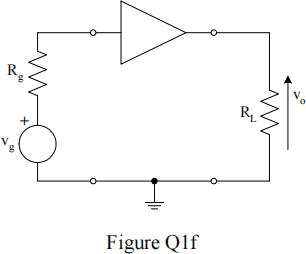
![]() f) The triangular element in the circuit shown in Figure Q1f represents an ideal current amplifier with a gain of 100. Work out the value of the voltage gain if Rg = 1 kΩ and RL = 15 kΩ .
f) The triangular element in the circuit shown in Figure Q1f represents an ideal current amplifier with a gain of 100. Work out the value of the voltage gain if Rg = 1 kΩ and RL = 15 kΩ .
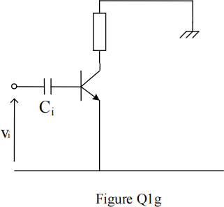
![]() g) Draw a mid-frequency ac equivalent circuit of the amplifier shown in Figure Q1g. (Note that bias and other components are omitted). Conduct an analysis to find a value for the capacitor, Ci to give a low-frequency roll-off point (- 3 dB) of 100 Hz. Which circuit capacitor is usually designed to set the low-frequency roll-off point in common-emitter amplifiers and why?
g) Draw a mid-frequency ac equivalent circuit of the amplifier shown in Figure Q1g. (Note that bias and other components are omitted). Conduct an analysis to find a value for the capacitor, Ci to give a low-frequency roll-off point (- 3 dB) of 100 Hz. Which circuit capacitor is usually designed to set the low-frequency roll-off point in common-emitter amplifiers and why?
The ac current gain, βO = 100 and the circuit is biased at IC = 0.1 mA.
![]() h) An operation amplifier with a slew-rate limit of 1 V/us is required to amplify a sinusoidal 100 kHz signal. Calculate the maximum amplitude of the output voltage that can be achieved without distortion. What type of output waveform distortion is seen when slew rate occurs and why? (consider a 741 op-amp)
h) An operation amplifier with a slew-rate limit of 1 V/us is required to amplify a sinusoidal 100 kHz signal. Calculate the maximum amplitude of the output voltage that can be achieved without distortion. What type of output waveform distortion is seen when slew rate occurs and why? (consider a 741 op-amp)
Total 40
2. The figure below shows a Widlar current mirror to generate the dc current, IO.

a) Neglecting base currents and assuming T1 and T2 are identical transistors, derive the design equation for the current IO, as given by:

where VT = kT/q; the symbols have their usual meanings.
b) The current mirror is required to provide the bias for a differential amplifier with resistor loads, RC1 = RC2 = RC. Sketch the circuit in your answer book. Design the circuit (calculate all resistor values) to give a DC bias current (in T2 above) of IO = 0.1 mA and DC output voltages of the differential amplifier of 0 V.
VCC = 10 V, VEE = – 10 V. Hint: allow 4VT = 100 mV across RE.
c) Draw the ac small-signal equivalent circuit of the amplifier and hence estimate the differential voltage gain. Explain any approximations and assumptions used in your calculations.
d) Comment on the expected magnitude of the common-mode rejection ratio. Explain your reasoning.
Total 20
3. Figure Q3 shows an operational amplifier circuit.
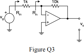
a) Identify the feedback topology and hence the amplification property that is stabilised by the feedback. Derive an expression for voltage gain of the amplifier assuming an ideal op-amp.
b) Sketch the equivalent circuit and hence work out a value for the loop gain, T of the amplifier for the following op-amp parameter values: differential input resistance, rd = 10 kΩ, output resistance, ro = 1 kΩ and open-loop gain, Aol = 103.
c) Hence work out a value for the input (Rn in Figure Q3) and output resistance. Is this a good op-amp? Explain your reasoning.
[Recall that Rout = ![]() and Rn =
and Rn = ![]() where Rf is the feedback resistor.]
where Rf is the feedback resistor.]
Total 20
4. a) List the advantages and disadvantages of the use of negative feedback in electronic systems.
b) Draw a block diagram of an amplifier with feedback, labelling clearly the open loop gain, Aol and feedback fraction, β. Show that the gain with feedback is given by;
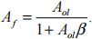
Under what conditions is the closed loop gain insensitive to variations in the open loop gain?
c) Figure Q4c shows an amplifier with feedback.
i) Identify the feedback topology and hence the type of amplifier.
ii) Represent the circuit as a negative feedback system and hence estimate the appropriate gain, assuming that the open-loop gain of the amplifier is large Consider the open-loop gain and use the equations given in the ‘amplifier properties’ page to justify the assumption.
Total 20

2023-08-28