ELEC 271 ELECTRONIC CIRCUITS AND SYSTEMS SECOND SEMESTER EXAMINATIONS 2017/18
Hello, dear friend, you can consult us at any time if you have any questions, add WeChat: daixieit
ELEC 271
SECOND SEMESTER EXAMINATIONS 2017/18
ELECTRONIC CIRCUITS AND SYSTEMS
![]() 1. a) Draw small-signal ac equivalent circuits of bipolar and MOSFET transistors at mid-frequencies, as defined between the two -3 dB points. Compare and contrast the ac parameters for transconductance and output resistance for application in analogue circuits.
1. a) Draw small-signal ac equivalent circuits of bipolar and MOSFET transistors at mid-frequencies, as defined between the two -3 dB points. Compare and contrast the ac parameters for transconductance and output resistance for application in analogue circuits.
b) Sketch a typical frequency response curve (Bode plot of voltage gain versus frequency) of an ac-coupled common-emitter voltage amplifier. Explain the form of the curve, indicating clearly the reasons for the low and high frequency roll-off.
c) Figure Q1c) shows a transistor amplifier circuit in which the quiescent DC collector current is 1 mA. Assuming that parameter rce and resistor RE are large enough to be neglected, draw the equivalent circuit and calculate the voltage gain, vo/vi. State an application for this amplifier. The collector resistor, RC = 2 kΩ .

![]() d) Figure Q1d) shows a simplified diagram of a cascode amplifier. Consider it as a two-stage amplifier and hence show, using the amplifier properties provided at the end of this paper, that the voltage gain is approximately given by;
d) Figure Q1d) shows a simplified diagram of a cascode amplifier. Consider it as a two-stage amplifier and hence show, using the amplifier properties provided at the end of this paper, that the voltage gain is approximately given by;

What is the main application for this amplifier?

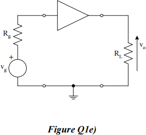
![]() e) The triangular element in the circuit shown in the Figure Q1e) represents an ideal trans-resistance amplifier with a gain of 100 kΩ. Work out the value of the voltage gain, vo / vg if Rg = 5 kΩ and RL = 10 kΩ .
e) The triangular element in the circuit shown in the Figure Q1e) represents an ideal trans-resistance amplifier with a gain of 100 kΩ. Work out the value of the voltage gain, vo / vg if Rg = 5 kΩ and RL = 10 kΩ .
![]() f) Figure Q1f) shows the ac equivalent circuit of a common-source amplifier where Rt is the ac load. The low-frequency roll-off is to be set by the capacitor CS. Design the amplifier to have a low-frequency roll-off, fL = 100 Hz. You may assume that RS is much greater than the impedance of CS at the frequency of 100 Hz. (gm = 1 mA/V)
f) Figure Q1f) shows the ac equivalent circuit of a common-source amplifier where Rt is the ac load. The low-frequency roll-off is to be set by the capacitor CS. Design the amplifier to have a low-frequency roll-off, fL = 100 Hz. You may assume that RS is much greater than the impedance of CS at the frequency of 100 Hz. (gm = 1 mA/V)

![]() g) The op-amp in Figure Q1g) is ideal. For the condition R1 = R2, show that the
g) The op-amp in Figure Q1g) is ideal. For the condition R1 = R2, show that the
output voltage, Vo is given by, vo = vg1+ vg2 .
How would you modify the circuit to obtain a gain of 10?
State all assumptions used in your analysis.![]()

![]() h) Explain the meaning of the terms, ‘voltage offset’ and ‘offset current’, in relation to operational amplifiers. How would you alleviate these problems for the caseof the inverting operational amplifier circuit?
h) Explain the meaning of the terms, ‘voltage offset’ and ‘offset current’, in relation to operational amplifiers. How would you alleviate these problems for the caseof the inverting operational amplifier circuit?
Total 40
2. You are required to design a common emitter voltage amplifier (find values for the resistors) to meet the following specification and criteria: a collector current of IC = 1 mA, DC voltage rail, VCC = 10 V and VBE(on) = 0.6 V.
a) Sketch the schematic circuit and calculate the four resistor values, RC, RE, RB1 and RB2 to meet the required specification, according to the following guidelines:
i) Allow 10% of VCC across RE,
ii) about 0.5 VCC at the collector node,
iii) the current in the base bias resistors should be ten times greater than the DC base current, where the DC current gain is 200.
Comment on each guideline.
b) The voltage gain of your amplifier is required to be greater than 50. Write down an expression for the voltage gain (see attached Amplifier Properties sheet) and hence find the minimum value of load resistor, RL that could be used, to satisfy this requirement.
Total 20
3. Figure Q3 shows a differential amplifier with current source biasing.
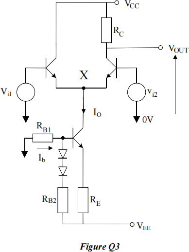
a) Explain the good features of this design.
b) Design the circuit (estimate values for the resistors) to meet the following specification: IO = 1 mA and the DC level at VOUT = 0 V.
Hints: Allow 2 V across RE, the current in the bias circuit, Ib = 0.1 × IO and the forward-bias diode drop is 0.6 V. You may assume ideal transistors with high DC current gain, with VCC = 10 V, and VEE = −10 V.
![]() c) Explain why point ‘X’ can be considered an ac ground for differential signals and hence draw an ac equivalent circuit for the differential amplifier. Use the equivalent circuit to estimate the differential gain.
c) Explain why point ‘X’ can be considered an ac ground for differential signals and hence draw an ac equivalent circuit for the differential amplifier. Use the equivalent circuit to estimate the differential gain.
Total 20
4. a) List the advantages and disadvantages for the use of negative feedback in electronic systems.
![]() b) Draw a block diagram of an amplifier with feedback, labelling clearly the open loop gain, Aol and feedback fraction, β. Show that the gain with feedback is given by;
b) Draw a block diagram of an amplifier with feedback, labelling clearly the open loop gain, Aol and feedback fraction, β. Show that the gain with feedback is given by;

Under what conditions is the closed loop gain insensitive to variations in the open loop gain?
c) Figure Q4 shows the circuit of an amplifier with feedback, partially prepared for ac. analysis by removing the large bias resistors, coupling capacitors and shorting out the DC supply.

i) Identify the feedback topology and hence the amplifier type.
ii) Represent the circuit as a negative feedback system and hence estimate the
appropriate gain, assuming that the open-loop gain of the amplifier is large.
State any approximations and assumptions used in your analysis. RF = 25 kΩ, andRE = 2.2 kΩ .
Total 20
2023-08-28