ELEC 271 ELECTRONIC CIRCUITS AND SYSTEMS SECOND SEMESTER EXAMINATIONS 2022/23
Hello, dear friend, you can consult us at any time if you have any questions, add WeChat: daixieit
ELEC 271
SECOND SEMESTER EXAMINATIONS 2022/23
ELECTRONIC CIRCUITS AND SYSTEMS
![]() 1. a) Sketch a typical frequency response curve (Bode plot of voltage gain versus frequency) of an ac-coupled common-emitter voltage amplifier. Explain the form of the curve, indicating clearly the reasons for the low and high frequency roll-off.
1. a) Sketch a typical frequency response curve (Bode plot of voltage gain versus frequency) of an ac-coupled common-emitter voltage amplifier. Explain the form of the curve, indicating clearly the reasons for the low and high frequency roll-off.
b) You are required to design a 2-stage voltage amplifier (find values for RE, RC1, RC2) to meet the following criteria: an input resistance of 500 kΩ and an overall voltage gain equal to or greater than 300, with a resistor output load, RL.
Use a common-emitter with emitter degradation (RE) stage for the input, followed
by a common-emitter amplifier with bias current equal to 0.75 mA.
(VCC = 15 V, βo = 250 and the DC levels of the first and second stage outputs need to be set at half the supply voltage. Allow 10% of VCC across RE). Proceed as follows:
i) Draw a schematic circuit of your amplifier, omitting the bias resistors and coupling capacitors.
ii) Work out the bias current and emitter resistor value to meet the input resistance specification. Hence find the value of the collector resistor of the first stage.
iii) Workout the gain of the first stage and hence find the required gain of the 2nd stage to meet the specification.
iv) Estimate the minimum value of load resistance, RL to satisfy the specification of voltage gain.
c) From the amplifier designed in 1b), comment on the ‘quality’ of your voltage amplifier and suggest how it could be improved.
Total 25
2. a) Draw small-signal ac equivalent circuits of bipolar and MOSFET transistors at mid-frequencies, as defined between the two -3 dB points. Compare and contrast the ac parameters for transconductance and output resistance for application in analogue circuits.
![]() b) Figure Q2b shows a differential amplifier with current source biasing.
b) Figure Q2b shows a differential amplifier with current source biasing.
Explain the good features of this design.
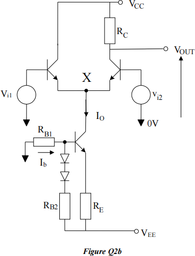
c) Design the circuit in Figure Q2b (estimate values for the resistors) to meet the following specification: IO = 1.5 mA and the DC level at VOUT = 0 V.
Hints: Allow 2 V across RE, the current in the bias circuit, Ib = 0.1× IO and the forward-bias diode drop is 0.6 V. You may assume ideal transistors with high DC current gain, with VCC = 15 V, and VEE = −15 V.
d) Give aphysical description of the terms ‘differential mode gain’ and ‘common mode gain’ with reference to the Figure Q2b.
e) Draw anac equivalent circuit for the differential amplifier. Use this circuit to estimate the differential gain.
Total 25
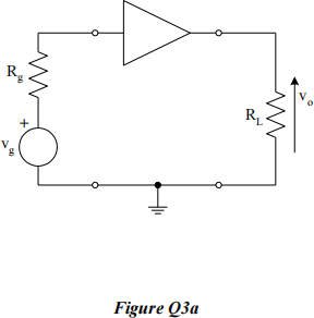
![]() 3. a) An ideal transconductance amplifier is connected as shown in Figure Q3a. The overall voltage gain of the circuit, vo/vg is 500 when RL is 10 kΩ. Calculate the gain of the ideal transconductance amplifier.
3. a) An ideal transconductance amplifier is connected as shown in Figure Q3a. The overall voltage gain of the circuit, vo/vg is 500 when RL is 10 kΩ. Calculate the gain of the ideal transconductance amplifier.
b) State the advantages and disadvantages of negative feedback.
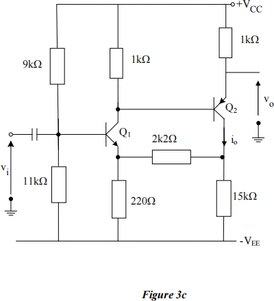
c) Identify the feedback topology of the amplifier shown in Figure Q3c and hence the amplifier type. Represent the circuit as a negative feedback system and hence estimate the appropriate gain.
State any approximations used in your analysis.
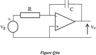
4. a) Design the operational amplifier circuit of Figure Q4a to have an input resistance of 20 kΩ and a time constant (R × C) of 15 µs. What function does the circuit perform?
![]() b) Draw an appropriate equivalent circuit for the amplifier shown in Figure Q4b, and hence derive the following expression for the input impedance.
b) Draw an appropriate equivalent circuit for the amplifier shown in Figure Q4b, and hence derive the following expression for the input impedance.
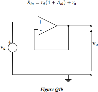
![]() c) Derive the following expression for the loop gain of the amplifier in Figure Q4b .
c) Derive the following expression for the loop gain of the amplifier in Figure Q4b .
Estimate values for T, β, Rin and comment on the values obtained.
Assume Parameter values are rd = 10 kΩ, ro = 50 Ω and Aol = 105.
d) Explain the meaning of the terms, ‘voltage offset’ and ‘offset current’, in relation to operational amplifiers. How would you alleviate these problems for the case of the inverting operational amplifier circuit?
Total 25
2023-08-25