ELEC 271 ELECTRONIC CIRCUITS AND SYSTEMS SECOND SEMESTER EXAMINATIONS 2021/22
Hello, dear friend, you can consult us at any time if you have any questions, add WeChat: daixieit
ELEC 271
SECOND SEMESTER EXAMINATIONS 2021/22
ELECTRONIC CIRCUITS AND SYSTEMS
1 a) Write down the equation that relates the collector current of the bipolar transistor to the base-emitter voltage. Hence prove the relationship gmrbe = βowhere the ac parameters are transconductance, base-emitter resistance and ac current gain respectively.
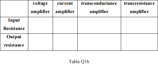
b) Copy table Q1b) into your answer book. Complete the table with the words ‘infinite’ or ‘zero’, to specify the values of input and output resistances for the four generic types of amplifier. All amplifiers can be considered ideal.
c) Draw a schematic diagram of a simple current mirror circuit. Show how it can be extended to form a current repeater. How can the current repeater be improved to allow different bias currents to be realised?
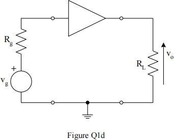
d) The triangular element in the circuit shown in Figure Q1d) represents an ideal current amplifier with a gain of 150. Workout the value of the voltage gain if Rg = 2 kΩ and RL = 9 kΩ .
e) State the advantages and disadvantages of negative feedback on amplifiers.
Total 25
2 a) Draw the small signal equivalent circuit of a common-collector amplifier with an ac load Rt. Hence derive an expression for the voltage gain. Explain what is meant by ‘small signal’ .
b) Perform a simple initial design of an ac coupled common-emitter amplifier with four resistor biasing and an emitter by-pass capacitor, to have a voltage gain of about 100,
for the following conditions. Justify any approximations used.
i) Transistor ac common-emitter gain, βo = 200
ii) Supply voltage of VCC = 15 V
iii) Allow 10% VCC across RE
iv) DC collector voltage of 10 V
v) DC current in the base bias resistors should be ten times greater than the DC base current.
Assume VBE(on) = 0.6 V. The load resistor, RL = 1.5 k Ω .
(Hint: first find a value for the collector resistor.)
c) Estimate a value for the input capacitor, CIN to set the low-frequency roll-off to be 1 kHz.
d) Which is the preferred way to set the low-frequency roll-off and how is this generally accomplished? What would be a practical value for CIN ?
e) What would be the next step in the design process?
Total 25
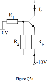
![]() 3 a) What is the function of the section of circuit shown in Figure Q3a).
3 a) What is the function of the section of circuit shown in Figure Q3a).
Calculate the value of Io, ifR2 = 4R1 and RE = 7.3 kΩ
b) Figure Q3b) shows a differential amplifier where the transistors can be considered to
be identical. The voltage gain is given by 
and VT = 25 mV.
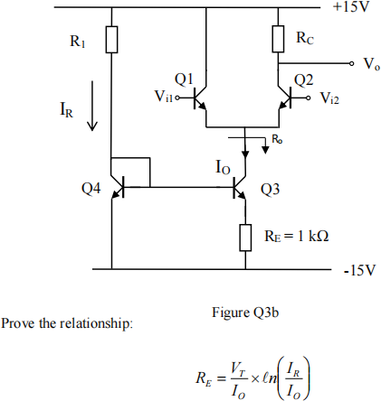
and hence design the amplifier (estimate values for resistors R1 and RC ) to give a voltage gain > 150 and a DC voltage level at the output of 0 V (Hint: allow 4 × VT across RE). What is the differential input resistance of the amplifier?
c) Explain the meaning of the term ‘common-mode rejection ratio (CMRR)’. Comment on the dynamic resistance (RO) looking into the current mirror and explain its significance for the CMRR.
d) Suggest how the design might be improved to make a better voltage amplifier.
Total 25
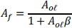
![]() 4 a) Draw the block diagram of a simple negative feedback system. Define the terms: open loop gain, Aoℓ , feedback fraction, β and closed loop gain, Af. Hence show the expression for the closed loop gain is given as:
4 a) Draw the block diagram of a simple negative feedback system. Define the terms: open loop gain, Aoℓ , feedback fraction, β and closed loop gain, Af. Hence show the expression for the closed loop gain is given as:
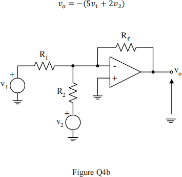
b) Calculate an expression for vo for the amplifier shown in Figure Q4b), assuming that the operational amplifier is ideal.
If the resistor Rf is chosen to be 22 kΩ, design the amplifier (estimate values for R1 and R2), in order to make:
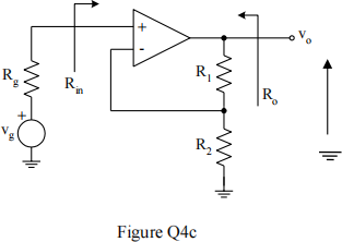
![]() 4 c) In the circuit shown in Figure Q4c), the operational amplifier has an input resistance, rd = 1 MΩ, an output resistance of 100 Ω and open loop gain (AOL) of 104. Assuming that Rg = 1 MΩ, R1 = 20 kΩ, R2 = 2 kΩ, estimate the loop gain (AOLβ, where β is the feedback fraction) of the circuit and hence find values for the input and output resistance Rin and Ro.
4 c) In the circuit shown in Figure Q4c), the operational amplifier has an input resistance, rd = 1 MΩ, an output resistance of 100 Ω and open loop gain (AOL) of 104. Assuming that Rg = 1 MΩ, R1 = 20 kΩ, R2 = 2 kΩ, estimate the loop gain (AOLβ, where β is the feedback fraction) of the circuit and hence find values for the input and output resistance Rin and Ro.
2023-08-25