ELEC 271 ELECTRONIC CIRCUITS AND SYSTEMS SECOND SEMESTER EXAMINATION 2019/20
Hello, dear friend, you can consult us at any time if you have any questions, add WeChat: daixieit
ELEC 271
SECOND SEMESTER EXAMINATION REPLACEMENTS 2019/20
ELECTRONIC CIRCUITS AND SYSTEMS
![]() 1. a) Draw the mid-frequency, small-signal equivalent circuit for a bipolar transistor, labelling clearly the parameters. Workout values for the parameters, gm, rce andrbe (the parameters have their usual meaning). The DC collector current is 1 mA; ac current gain, βo is 100 and the Early voltage, VA is 100 V.
1. a) Draw the mid-frequency, small-signal equivalent circuit for a bipolar transistor, labelling clearly the parameters. Workout values for the parameters, gm, rce andrbe (the parameters have their usual meaning). The DC collector current is 1 mA; ac current gain, βo is 100 and the Early voltage, VA is 100 V.
b) Figure Q1b shows an amplifier circuit where bias resistors are omitted. Identify the amplifier type and hence design it to have a voltage gain of 10.

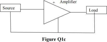
![]() c) Figure Q1c shows an amplifier system. The source has a small internal impedance and the load is a small resistance. Choose a suitable amplifier type to ensure good matching between source and load. Hence sketch a systems diagram with appropriate equivalent circuits for the source (Thevenin or Norton) and generic amplifier type.
c) Figure Q1c shows an amplifier system. The source has a small internal impedance and the load is a small resistance. Choose a suitable amplifier type to ensure good matching between source and load. Hence sketch a systems diagram with appropriate equivalent circuits for the source (Thevenin or Norton) and generic amplifier type.
d) Work out the dc voltage levels of the circuit of Fig. Q1d and hence find values for IC(Q1), IC(Q2), IR1, IR2 .
Assume that VBE (on) = 0.6 V and dc base currents can be assumed negligible.

e) Compare and contrast the use of bipolar and MOSFET transistors in analogue circuits.
f) How would you design a near ideal voltage amplifier incorporating negative feedback? What would be the advantages and disadvantages of your design compared to a voltage amplifier without negative feedback?
g) Design the operational amplifier circuit of Figure Q1g to have an input resistance of 10 kΩ and a time constant (R × C) of 10 µs. What function does the circuit
perform?

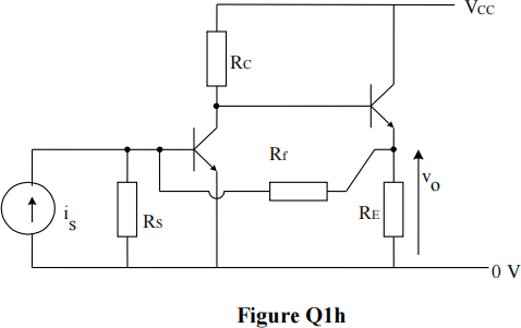
h) Figure Q1h shows a schematic diagram of a feedback amplifier with bias components removed. Identify the feedback topology and the amplifier type.
Hence write down an expression for the feedback fraction, β .
2. a) Perform a simple initial design of an ac coupled common-emitter amplifier with four resistor biasing and emitter by-pass capacitor, to have a voltage gain of about 100, for the following conditions. Justify any approximations used.
i) Transistor ac common-emitter gain, βo = 100 and dc gain is also 100.
ii) Supply voltage of VCC = 20 V.
iii) Allow 10% VCC across RE.
iv) DC collector voltage of about VDD /2.
v) DC current in the base bias resistors should be ten times greater than the DC base current.
Assume VBE(on) = 0.6 V. The load resistor, RL = 1 k Ω .
(Hint: first find a value for the collector resistor.)
b) Estimate a value for the input capacitor, CIN to set the low-frequency roll-off to be 1 kHz.
c) Which is the preferred way to set the low-frequency roll-off and how is this generally accomplished? What would be a practical value for CIN?
d) What would be the next steps in the design process?
Total 20
3. Figure Q3 shows a differential amplifier where the transistors can be considered to be
identical. The voltage gain is given by 

a) Prove the relationship:

stating assumptions made in the derivation. Hence design the amplifier (estimate values for resistors R and RC ) to give a voltage gain > 100 and a DC voltage level at the output of 0 V (Hint: allow 4 × VT across RE). What is the differential input resistance of the amplifier?
b) Explain the meaning of the term ‘common-mode rejection ratio (CMRR)’. Comment on the dynamic resistance (RO) looking into the current mirror and explain its significance for the CMRR.
c) Suggest how the design might be improved to make a better voltage amplifier.
Total 20
4. a) Explain what is meant by the virtual short principle as applied to operational amplifiers with negative feedback.
b) Draw an appropriate equivalent circuit for the amplifier shown in Figure Q4b, and hence derive the following expression for the input impedance.
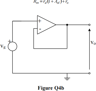
c) Derive the following expression for the loop gain of the amplifier in section b).

Estimate values for T, β,Rin and comment on the values obtained.
Parameter values are rd = 10 kΩ, ro = 50 Ω and Aol = 105.
Total 20
2023-08-25