ECS517U Electronic Devices and Applications 2017
Hello, dear friend, you can consult us at any time if you have any questions, add WeChat: daixieit
DATE 2017 TIME TBD
ECS517U Electronic Devices and Applications Duration: 2 hours 30 minutes
Question 1
a) This question concerns the properties of diodes.
i. Sketch the current-voltage characteristic of a model of (1) an ideal diode and (2) a real diode. Clearly annotate all relevant points on the graph. [2 marks]
ii. Give values for reverse saturation current and conduction voltage for a typical low-power silicon diode. [2 marks]
b) Consider the diode circuit as shown in Figure Q1.b. The diode conduction voltage of both diodes is 0.7V, and the Zener reverse breakdown voltage is 5V. Resistors R1 and R2 have values R1 = R2 =1kOhm.
i. Analyse operation of the circuit and determine its transfer function. That is, find mathematical expression for Vo as a function of Vi. [4 marks]
ii. Sketch the graph of the transfer function, i.e. of how the output voltage Vo
depends on the input voltage Vi.. Label the x and y axes clearly in your graph, and annotate all the relevant points. [3 marks]
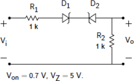
Figure Q1.b
iii. Assuming Vi (t) = 6 cos(ot) V, plot Vi (t) and Vo (t) on the same graph. Label the axes clearly, including the axes units. [4 marks]
c) Figure Q1.c shows a regulated 12V power supply. Transformer rating is
expressed as r.m.s. values. Diodes D1-D4 have conduction voltage of 0.7V, while D5
is a Zener diode, with the rating as given in the figure. This DC power supply provides power to a load that draws a maximum current of 100mA.
Determine the range of possible values for resistor R1 and its minimum power rating requirement. [10 marks]
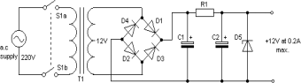
Figure Q1.c.
Question 2
A displacement sensor drives a DC servo-motor via an amplifier. The displacement sensor has a sensitivity of 1mV/mm. The system is calibrated so that at 0mm displacement from a set point, the DC motor is stationary at an angle of 0 rad. When a non-zero displacement is measured, DC servo motor rotates to produce angular displacement θ [deg]. 1mm linear displacement corresponds to angular displacement of DC motor of 1 deg. An amplifier takes the signal from the sensor and converts it to a form suitable for driving a motor.
The output resistance of the sensor sub-system is 200Ω. The motor has an input resistance of 2kΩ, and an input voltage to the motor of 20V produces one full revolution of the DC motor. The amplifier subsystem has an input resistance of 2kΩ and an output resistance of 100Ω. The open circuit voltage gain Av may be adjusted over a wide range of values, as required.
a) Sketch the equivalent circuit of this system. [5 marks]
c) Derive an expression for a relative reduction in gain ΔAv due to loading effects, in Av
the general case of a real amplifier. Then calculate the relative change in gain, expressed as a percentage, for the system given in the question, above. [10 marks]
Question 3
a) Sketch the equivalent circuit of an ideal op-amp and outline its characteristics.
Then, sketch the equivalent circuit of a typical real amplifier and explain how it differs from the ideal op-amp model. [5 marks]
b) Sketch a block diagram of a generalized feedback system and derive an
expression for the output in terms of the input, Vi , the gain of the forward path, A, and the gain of the feedback path, B.
Under what condition does this arrangement produce negative feedback?
If the forward gain of a system with feedback is A= 100, and the feedback gain is B =
-0.011, determine whether the feedback is positive or negative. What are the potential issues with this system? [8 marks]
c) Design an inverting amplifier with an overall gain of -100. Your initial analysis can assume an ideal op-amp characteristics, but the final choice of resistor values should be based on typical 741 characteristics. Sketch the circuit diagram and justify your
choice of resistor values. [7 marks]
d) For the inverting amplifier you designed in part (c) estimate the bandwidth, input resistance, and output resistance, based on typical parameters for a 741 op-amp, if the unity bandwidth-gain product is 1,000,000. [5 marks]
Question 4
a) Design an amplifier using the common-emitter configuration shown in Figure
Q4.a, with a bias that would maximise the output voltage swing and minimise
potential for clipping and distortion. That is, determine the values of the RB and RC. Briefly justify the choice of your output voltage quiescent point.
The amplifier will use a supply voltage of VCC=10V. The quiescent collector current should be around ICQ=1mA. The resistor in the emitter has a value of RE = 1kOhm. Current gain of the transistor is hFE = 200. [10 marks]
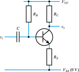
Figure Q4.a
b) Figure Q4.b shows a single-supply amplifier with feedback and “stiff base” bias. The collector and base resistors have values: RC = 10 kΩ, RB = 830 kΩ, and the
supply voltage +Vis 10V.
What values should the resistors R1 , RE and the capacitor C1 have, such that the small-signal gain is -10, the quiescent output voltage is Vo = 5V, and the low-frequency cut-off is 200 Hz ? [10 marks]
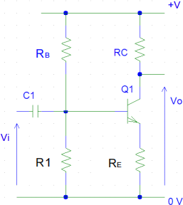
Figure Q2.b
c) Sketch atypical transfer characteristics for a DE-MOSFET, clearly marking the region of the normal operating range on the sketch. Then explain the role of the resistor RG in the circuit of Figure Q4.c. [5 marks]
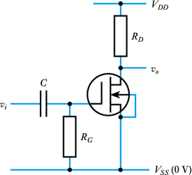
Figure Q4.c
2023-08-21