Building a MIPS Processor
Hello, dear friend, you can consult us at any time if you have any questions, add WeChat: daixieit
Building a MIPS Processor*
(*Well, a slightly simplified version that only supports the instructions lw, sw, beq, add, sub, and, or, and slt instructions.)
Introduction
In this lab you will do three things:
1. Define the control logic for the datapath control signals
2. Hookup the key parts of a MIPS processor to make a working datapath. 3. Verify that your design works by running a simple program
What to turn in
1. You are expected to turn in your completed mips-datapath-lab.circ file. You should rename it as: “ lastname-firstname-mips-datapath-lab.circ” before you turn it in to simplify grading.
2. You are also required to turn in a pdf file in which you answer the ToDos found within this document (name is as “ lastname-firstname-mips-datapath-lab.pdf”).
Getting Started
Read the background material
Before you get started, we strongly recommend you read chapter 4.3 and 4.4 in the 5th edition of the book (Patterson & Hennessy, Computer Organization and Design: The Hardware/Software Interface). This will both show you pictures of what you are to build and explain how it works.
Files and programs
You are provided with the following files in the mips-datapath-lab.zip archive:
. mips-datapath-lab.circ: an eviscerated shell that is missing all the important parts of a MIPS processor
. 1234.mem: a hex memory file that contains the values 1, 2, 3, 4 in the first 4 words of memory
. test-code.mem: a file that contains a simple test program for verifying your design
To use these files you will need to install Logisim on your computer. We trust that you are capable of using Google to figure this out. Note that you may have to install a Java runtime to run Logisim. This is quite safe as long as you do not enable Java in your web browser.
Using Logisim
We recommend you watch the Logisim tutorials online before starting this lab (check this one for example). The key things for you to know before starting are:
1. How to wire up components in Logisim (drag with the arrow cursor) and how to add logic gates (click on them under “Gates” on the left).
2. How to edit the insides of components in logisim (double-click) and go back to the top view (click on “mips” on the left).
3. How to simulate in Logisim (choose “Simulation Enabled” and use the pointer cursor to change values).
4. How the clock works in Logisim (choose “Tick Once” to execute one clock cycle).
Take a look at what we provided:
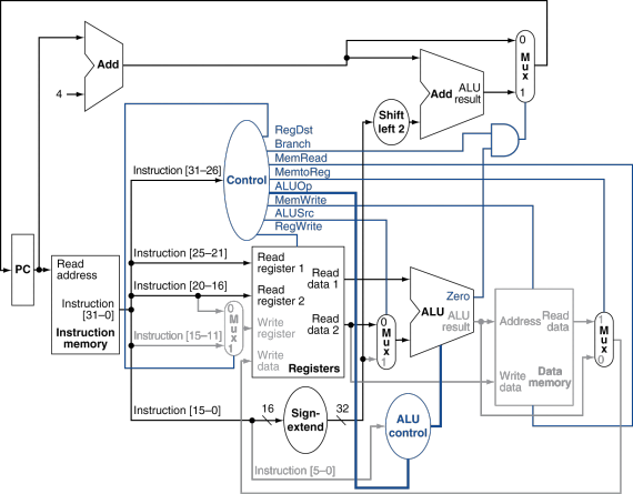
Open the mips-datapath-lab.circ file. You’ll see something that looks a lot like the figure in the book:
Processor from the book and lectures:
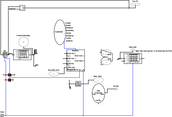
What you get:
Okay, so maybe they don’t look all that similar, but you should be able to identify the same overall shape (the big loop on the top is part of the next PC logic) and the key components: PC, instruction memory, control logic, registers, ALU control, ALU, and data memory.
You probably noticed that the only wires we’ve included for you are the clock (at the bottom), a simplified next PC logic path (at the top), resets for the PC and register files (the red buttons), and one hint for getting started: we hooked up the RegWrite output from the Control logic to the RegWrite input on the Register file. (Wasn’t that nice of us?) There are also several MUXes missing. Completing the datapath connections is the second part of this lab.
The first part of the lab is completing the control logic. That’s right: those lovely ovals labeled “Control” and “ALU Control” are not finished on the inside. You will need to figure out the logic that goes inside of them.
A closer look
Before we get started on the actual work for the lab, let’s take a slightly closer look at what you have. Right-click on the ALU and choose “View alu” or double-click on it in the hierarchy list on the left.
The ALU
Here you can see the ALU. It has two inputs (A and B) and calculates 6 functions:
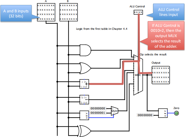
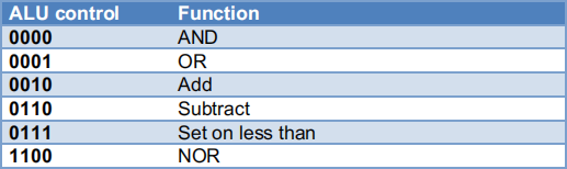
All 6 functions are calculated all the time, but the MUX at the end selects the right one based on the ALU control inputs. You can see from the figure that if the input to ALU control is 0010=2, then it will select input 2 (the third one since it starts counting at 0) and the output will be A+B. Compare this to the ALU function table below and make sure it makes sense to you. In particular, make sure you understand how the “set on less than” is implemented, since you will use that kind of logic later in the lab.
Now go back to the main view (double click on “mips” on the left) and then take a closer look at the “Control” unit.
The Control unit
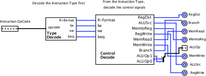
You can see that the control unit has 4 parts:
1. The input: the instruction OpCode
2. The “Type Decode” which takes in the OpCode and outputs whether the instruction is an R-format, lw, sw, or beq instruction.
3. The “Control Decode” which takes in the type of instruction and outputs the correct control signals for the datapath.
The Control unit’s job is to decode the instruction OpCode to control all the parts of the datapath. To do this we break up the decoding into two parts: first we decode the instruction type, then we use the instruction type to decode the control signals. This simplifies each piece of logic, which is great since you have to build them. (In practice, a CAD package will decide exactly how to break up the logic to make it as fast as possible.)
Part 1: Finishing the Control Logic
Now we’ll get down to the real work of making the control logic work. There are three parts you will need to complete: the Type Decode unit, the Control Decode unit, and the ALU Control unit. Each one uses a slightly different way to generate its output, so stay awake!
Start by taking a look inside the “Type Decode” unit:
The Instruction Type Decode Unit
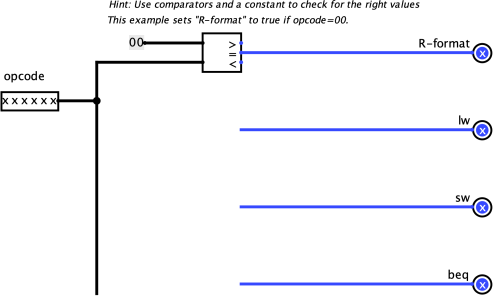
Here you see that this unit is not complete. You will need to complete it to finish the lab. However, there’s a hint about how to make this work. Notice how a comparator and a constant value are used at the top to determine if the instruction is R-format. What that logic does is determine if the OpCode equals 00. If it does, then the = output of the comparator will be true, and the R-format output of the block will be set to 1. Your job is to fill in the rest of this unit so it correctly asserts lw, sw, and beq when those types of instructions are encountered.

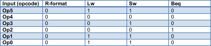
To determine the instruction type you need the following information:
Testing
Once you have built the circuit you need to test it. To do this choose “Simulation Enabled” from the Simulate menu and use the hand pointer to set the inputs and make sure the right output is activated. Below I clicked on all the OpCode bits to make them 0 (don’t worry about warnings that the state is set from elsewhere; that’s just saying this block is hooked up). When they were all 0, the R-format output became 1 (light green) as we expect. Test all four inputs.
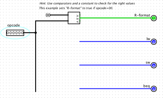
Testing the Type Decode Unit: I’ve put all zeros in the opcode input and it correctly enables only the R-format output.
The Control Decode Unit
Once you’ve completed the Instruction Type Decode unit you’ve got half of the Control logic finished. The other half is using the instruction type to determine the control signals to send. Take a look inside the control-decode unit to see what you’ve got to fill in there.
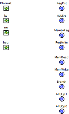
Well, this is what you’d expect: the inputs are the instruction type (on the left) and the control signals are the outputs (on the right). Now to generate this logic you can either stare really hard at the table below and figure it out yourself (which is fine) or you can use the built in “Combinatorial Analysis” tool in Logisim to build it for you.
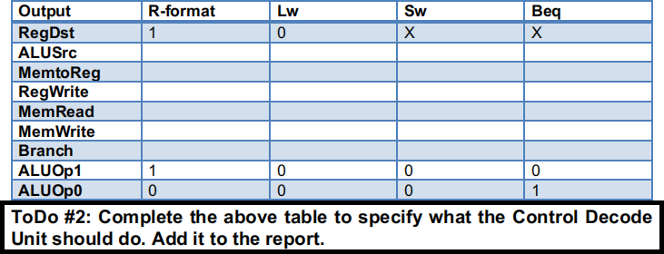
To do either, you need to know what the values should be. So, fill in the truth table below for each instruction type. Remember that you can (and should) put in an X for options that you don’t care about. To do this you should think about what each instruction does. If you just copy this from the book or online you will have a much harder time debugging later because you won’t understand as well.
Now that you’ve got the definition for the Control Decode Unit above, it’s time to build it. Either just stare at it and figure out the logic (it’s not that complicated) or use the Combinational Analysis tool under the Window menu.
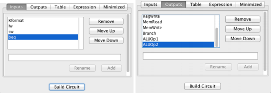
For the Combinational Analysis Tool you first need to define the Inputs and Outputs of your circuit. These are the row and column headers from your truth table above:
Then enter the values into the Table section. Remember that if you don’t care about a particular output you should just mark it as X. Click on the values to change them.
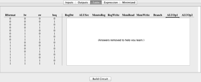
Now that you’ve done this, you can let LogiSim do all the hard work for you. Under “Expression” you can see the logic equations for each output, and under “Minimized” you can see the Karnaugh maps for each expression. To just have LogiSim build the circuit, click on “Build Circuit” and add it to the current project with name “control-solution” .
You’ll now see the solution circuit in LogiSim. However, you need to copy the logic over into the real “control-decode” circuit to make it work. (Hint: select all the gates and copy them into the old circuit, but make sure the wires line up and connect to the right outputs.)

Testing
Once you have built the circuit you need to test it. Do this the same way you did for the previous circuit and make sure that the correct signals are set for each type of instruction.
Congratulations! You’ve now built the full control logic and tested each component. However, we strongly recommend you test the full thing. To do so, go to the control circuit and test the whole chain. E.g., put inputs into the Instruction OpCode and verify that the correct control signals are set at the output. (Trust me: time spent testing is well worth it!)
The ALU Control Unit
Take a look inside the ALU control unit, but don’t be shocked. This unit has 8 inputs (2 ALUOp bits and 6 Function bits) so there are a lot of wires. In fact, it’s laid out rather nicely. The inputs all go vertically down the left side and the output is on the far right. The logic that connects the inputs to the outputs goes in the middle. Spend a few minutes to figure out what the part on the right is doing to generate the output before you read the next paragraph.
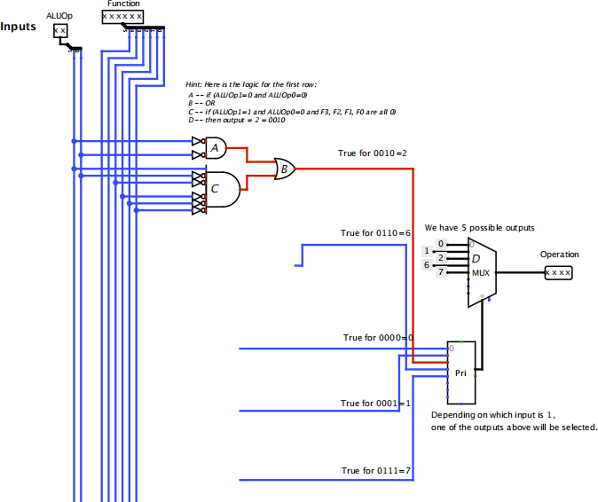
(You spent a few minutes pondering the logic on the right before reading this paragraph, right?)
If you look at the logic on the right, the output is coming from a MUX (D). The MUX has constant values as inputs (0, 1, 2, 6, and 7). The MUX is driven by a priority encoder (Pri), which takes signals from the logic in the middle. What happens is that if one of the inputs to the priority encoder is true, the priority encoder will tell the MUX to select that input, which will output the constant.
To make this all work, you just need to build the logic that determines which input to the priority encoder should be true given the ALUOp and Funciton inputs on the left.
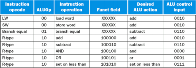
Also, ALU control bits based on ALUop and Func field are provided below:
The truth table for controlling the ALU is also shown below:
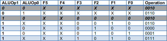
Notice the part we’ve already done for you in shading (the two combinations that give you a 0010 as the output). Try to write down what the logic should be for determining if the operation is 0010 before you read further. Look at the bits in the table and figure out what the conditions are.
(Really, try to do this before you read the next bit.)
Let’s take a look at the first row. We have:
. ALUOp1=0, ALUOp0=0, and all Fs are X. So the logic here is:
. Operation should be 0010 whenever ALUOp1=0 AND ALUOp0=0. (We don’t care about the Fs because they are Xs.)
Now look at the circuit that we gave you above:![]()
![]()
![]()
The top half (A) is an AND gate that is ANDing (NOT ALUOp1) and (NOT ALUOp0). This means the output of that AND gate will be true when ALUOp1=0 AND ALUOp0=0. (Which is, not so surprisingly, exactly what we want.)
Now what about the second shaded row where the answer is 0010? Try to work that out before going on.
The second row is:
. ALUOp1=0 AND ALUOp0=0 AND F3=0 AND F2=0 AND F1=0 AND F0=0
Now look at the rest of the circuit (C) we built for you:

This is exactly that!
Now we have two cases where the output should be 0010. We need a final OR gate (B) to make sure that the output will be 0010 if either is true:

The result of the OR gate is 1 whenever the output should be 0010. To make the output be 0010 that value goes into the priority encoder, which selects the right input from the MUX to send out the results.
Note that all of the entries have Xs for both F4 and F5. That means we never use their values. So if you find yourself wiring up either F4 or F5 here you’ve probably made a mistake.

Testing
Once you have built the circuit you need to test it. Do this the same way you did for the previous circuit and make sure that the correct signals are set for each type of instruction.
Part 2: Hooking Up the Datapath
Now that you’ve completed (and tested, right?) the control logic, it’s time to hook up the datapath. Use the figure from the book (or datapath lectures) and your understanding of how the MIPS processor works to complete the datapath we’ve provided. You should not delete anything we’ve put in there. (There are a whole bunch of “probes” that show you the values on wires which you’ll want for debugging.)
You will need to pay special attention to how the instruction is broken up for connecting the processor. Note how the output from the instruction memory is split into four parts and you can see which bits are in each part. Also note that another copy of the instruction is split up below for the immediate field. You need to make sure you know which part of the instruction goes where! You can click on the splitter to see how it is configured as well.
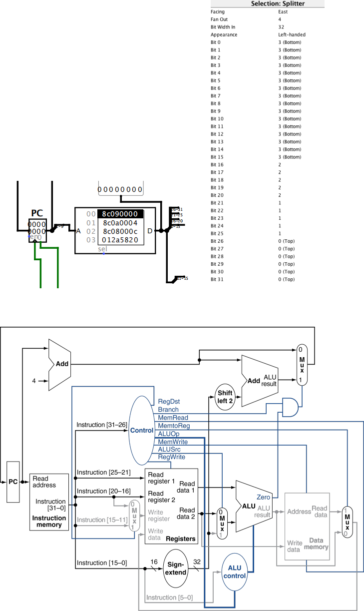
Above is a copy of the figure from the book on how the processor is hooked up. Make sure
you don’t get the MUXes backwards and don’t forget that the next PC logic isn’t correct in the version we gave you.

Testing it with Code
To test your processor we’ve provided you with the following program (test-code.mem):
lw $t1, 0($zero)
lw $t2, 4($zero)
lw $t0, 12($zero)
loop:
add $t3, $t1, $t2
add $t4, $t3, $t1
sub $t0, $t0, $t2
or $t5, $t4, $t1
slt $t6, $t4, $t5
beq $t2, $t0, loop
And a memory file that contains 1,2,3, and 4 in the first 4 words of the memory (1234.mem).
To use these files you need to right-click on the instruction memory and data memories and load the appropriate files.
Now before you start running the program, figure out what that code will do.
Write down for each cycle (until the program runs out of instructions) what value is in each used register and what value and register will be written to for each instruction. (This is incredibly helpful for debugging.)
Once you’ve figured out what the program will do and what value will be written back to the register file after each instruction, start your program. Enable simulation, click the “Reset Program” and “Zero Register File” buttons to clear them. And then choose “Tick Once” to advance through each instruction.
When you first start simulating your first instruction will be in the processor. Make sure everything is working. Check the inputs and outputs, the MUXes, the control bits. And finally, check that the value being written back into the register file and the register being written. (These are both displayed with probes in the file so you can see them as the processor runs.)
When your program runs out of instructions you can double-check the contents of the register file by opening it up.

Debugging tips
. Don’t advance past the first instruction until it is working correctly.
. Check that the values for all registers (selected register and data) are correct and that the ALU operation is correct.
. Use the finger tool to see the values on wires in the processor.
. Trace values back to the first place where they are wrong, and then go into that part to see what is going on.
. You can go inside the Control unit while your processor is simulating to see where mistakes are.
. You can view the contents of the register file by viewing inside it as well.
. Write out what you expect to happen and verify it. Don’t guess.
. When you need to restart the program click Restart Program AND click Zero Reg File.
. If you reset the simulation then the memory will be zeroed and you will have to re- load the memory data.
That’s it.
Turn in your completed project and the answers to the 6 ToDos. The TA/Graders will test your processor file and check your questions. Don’t turn in an overly messy design as the TA won’t be able to understand it and will deduct points.
Grading (total 14 points)
Part 1 (7 points)
. ToDo #1 (2 points): for the correct implementation of the unit and the screenshop in the report
. ToDo #2 (1 point): for the completed table
. ToDo #3 (2 points): for the correct implementation of the unit and the screenshop in the report
. ToDo #4 (2 points): for the correct implementation of the unit and the screenshop in the report
Part 2 (7 points)
. ToDo #5 (5 points): for the correct implementation of the processor and the screenshop in the report
. ToDo #6 (2 points): for the correct status of the register file after executing the program and the screenshot in the report
2023-08-12