ES3E0/ES4D4 Power Electronic Converters and Devices
Hello, dear friend, you can consult us at any time if you have any questions, add WeChat: daixieit
Assignment
Power Electronic Converters - Design and Experiment
2022-23 Resit
Module code and title: ES3E0 Power Electronics, ES4D4 Power Electronic Converters and Devices
Assessment setter (module tutor): Jihong Wang
Assignment Weighting and typical hours work: 30% weight, 45 hours
Learning outcomes assessed:
• Design and analyse a power converter, including an AC-DC converter, a DC-DC converter and apply mathematical modelling in analysis.
• With the aid of literature, explain the practical issues in converter design.
• Analyse the power quality and harmonics. Design the basic filters to smooth the converter output and to improve the power quality.
• Design and test a boost DC-DC converter and its associated control.
Context/Introduction/Background to the assignment and Requirements/Task:
There are two parts of tasks for this assignment:
AC-DC converter design and analysis
DC-DC converter design, test and analysis
The description and requirement of the tasks are specified and the lab script is included as an appendix.
Formatting requirements of report:
• The final report should cover the work for all the tasks specified in the assignment document. The requirements for what should be included in the report are explained in the assignment document.
• The word limit is 2000 (2000 words is a guideline, which should not stop you to present good quality work if you need to use more than 2000 words. Also, you do not have to use all 2000 words!). Make sure your report contains the necessary content, but please try to be concise.
• This is worth 30 % of the module.
Submission date/deadline:
The submission deadline is 12:00pm, 29 Aug 2023. Please check the deadline shown on tabula for exact time and date. All submissions that miss the deadline will be subject to the normal 5 marks per day penalty.
Assessment criteria/mark scheme:
Marking is out of 100% and the marking scheme is available on Moodle page.
1. AC-DC Converter Design and Analysis
1.1 You are required to design a single-phase full bridge diode AC-DC converter. The specifications are as follows:
- The input power is from the mains with the voltage of 230 VRMS and frequency of 50 Hz.
- The output DC voltage is 48 V with the maximum voltage ripple of 6 V. The output current rating is 5 A.
You are required to present the following in your report:
- a sketch of the converter circuit of your design
- the work out procedure for calculation and analysis of converter component values; the parameters and your chosen values and parameters of your design
- voltage and current ratings of the switching device diodes
- a sketch of the source current and voltage waveforms assuming that only capacitance smoother is adopted
- a sketch of the source current and voltage waveforms assuming that an Inductance and
Capacitance (LC) filter is used and the continuous current operation model is maintained. (15%)
1.2 Design a three-phase full bridge thyristor AC-DC voltage converter with the following design specifications:
- The input voltage is from the mains and the phase voltage varies between 190 to 230 VRMS ;
- DC output voltage required is 400 V and output current limit is 100 A;
- The converter is operating in a continuous load current mode.
You are required to present the following in your report:
- a sketch of the converter circuit of your design
- the range of thyristor firing angles
- voltage and current rating of the switching devices
- a sketch of the source current and voltage waveforms assuming that the load current is continuous
- with a firing angle at 300 and the phase voltage at 230 Vrms, find the minimum of L to maintain the load current ripple less than 10A. (20%)
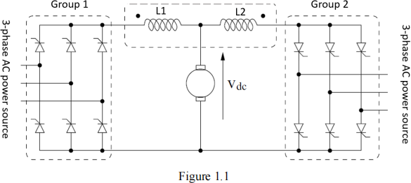
1.3 A typical thyristor rectifier for driving a DC motor is shown in Figure 1.1.
- Explain how the rectifier can power a DC motor to rotate in both directions.
- To increase the speed of the DC motor, should the firing angle be increased? Explain your answer.
- Explain what is going to happen if both Group 1 and Group 2 thyristors are fired to conduct at the sametime.
- Explain the role of inductances L1 and L2. Explain why the two inductances have the polarity arranged as shown in Figure 1.1.
(15%)
2. DC-DC Converter Design, Test and Analysis
The purpose of the coursework is to understand the design steps presenting in the design and testing of a DC-DC boost converter. This is linked to Boost Converter experimental work. You are required to understand and analyse the test results obtained from the experiments.
Before you start working on this coursework, you need to read the Boost Converter Lab script first, which is attached in the Appendix.
Design Specifications
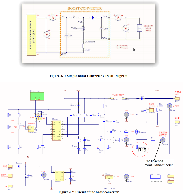
You are asked to design and test a boost (step-up) converter for converting 30 V DC to 48 V DC, shown in Figure 2.1. The output must be capable of driving a load of 100 W.
The specifications of the converter are:
• 30V DC input
• 48 V DC output
• 100 W output power
• Output voltage ripple is less than 200 mV pk-pk
In the design, you are to achieve the above specifications by selecting suitably-sized components from the nearest preferred values from the following list of capacitors and inductors.
Capacitor values:
100, 220, 330, 470, 1000, 2200 μF; all rated at a voltage of 63 V.
Inductor values (current ratings are max. average continuous current):
100 μH, 7.8A
150 μH, 6.5A
220 μH, 5.5A
330 μH, 4.5A
470 μH, 4A
Other assumptions for your design are:
• The boost converter will use continuous conduction.
• The MOSFET to be used is IRFI14110G, and diode to be used is UF5401.
• The switching frequency will be 25 kHz.
• The PWM controller is a LM3524.
Datasheets are available online on the module Moodle website for the IRFI4110G MOSFET and UF5401 diode.
The boost converter circuit topology is same as the one used in Lab test board. The circuit diagram and layout of the board are shown in Figure 2.1 and Figure 2.2.
Task 1.
i) Find the values of suitable inductor (L) and capacitors (Cout) to ensure the output voltage ripple is less than 200 mV pk-pk. Show all the design, work out procedure and analysis in the report. You should select suitably-sized components from the nearest preferred values listed in the section of the design specifications. (Mark 8 %)
ii) The input DC power is provided by a lab bench DC power supply as shown in Figure 2.3. From Figure 2.3, each channel has 3 A as its maximum output current.
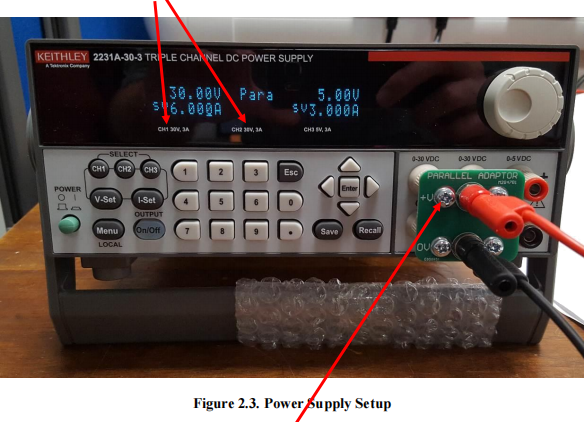
Explain why two channels connected in parallel to provide the output DC power? (Mark 2%)
Task 2.
i) Figure 2.4 shows the typical curves of VDS and VGS. Identify which curve represents VDS and which one represents VGS. From the curves shown in Figure 2.4, work out the switching frequency and the duty ratio.
(You may refer to the document “Using the Oscilloscope” that is available from Moodle Page.)

(Mark 8 %)
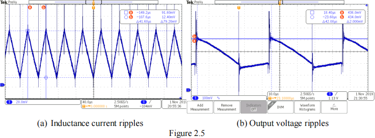
ii) The inductance current and output voltage curves are shown in Figure 2.5. Mark the switch “ON” and “OFF” time periods on both inductance current and output voltage curves.
(Mark 4%)
iii) Figure 2.6 shows a transient response of the boost converter output voltage, from which there is no overshoot in the response. Explain why the overshoot and oscillation may occur when the load changes.

(Mark: 4%)
iv) When the load is set as 0, some students find oscillations of the main switch. The waveforms of VDS and VGS are captured on the oscilloscope as shown in Figure 2.7. Explain why the oscillation happened.

(Mark: 4%)
Task 3.
The boost converter adopts an analogue PI controller and the PI controller circuit is shown in Figure 2.8 and circuit board is presented in Figure 2.9.
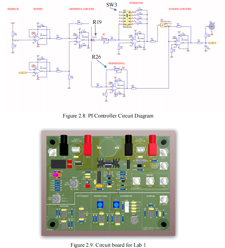
i) Explain how the PI controller used in this Lab can regulate the duty ratio and the boost converter output voltage to the desired value while the converter is subject to load changes and input voltage variations. (Mark: 8%)
ii) Figure 2.10 shows a transient response curve obtained from the experimental work when P-control is applied.
- Explain why the oscillation occurs in the dynamic responses with P control.
- Find the rising time from Figure 2.10.
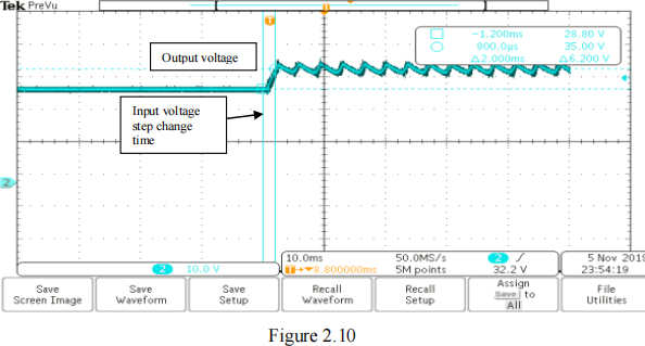
(Mark: 6%)
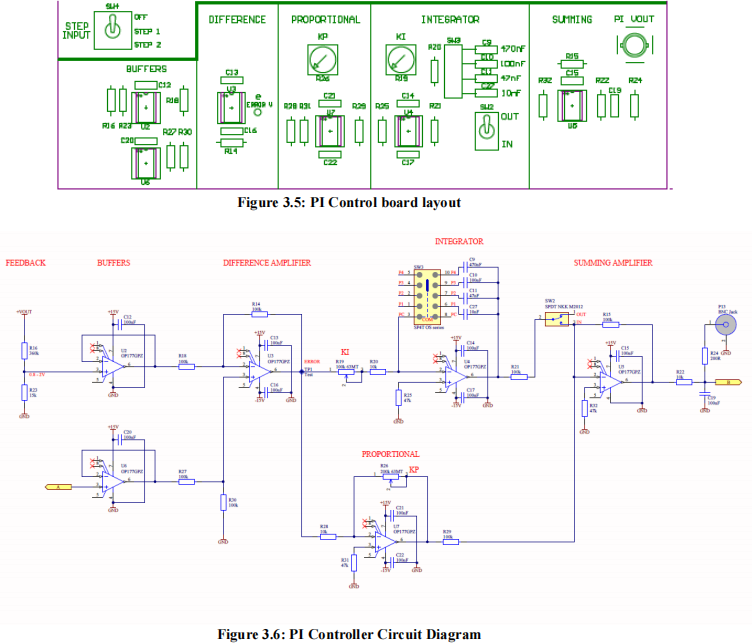
iii) When the student uses PI-control, one transient curve was captured and is shown in Figure 2.11. To reduce the oscillation, the proportional and integral gain should be reduced. With reference of Figure 2.8 and Figure 2.9, explain how adjusting R26 can reduce the proportional gain Kp and how adjusting R19 and SW3 setting can reduce the integral gain Ki of the PI controller.
(Reference Lecture 9)

(Mark: 6%)
Appendix (Lab Scripts)
DC-DC Converter Design and Specifications
(To complete the calculation of the suitable L and C components before your lab session.)
This task is to design a Boost Converter and then experimentally test the converter in the laboratory using your chosen component values and the experimental results will be compared to the predicted ones. In the experimental test, you will introduce a PI controller to form a closed-loop system control of the boost converter and then test its performance while it experiences load variations and the disturbances from the DC power source.
You are asked to design and test a boost (step-up) converter for converting 30 V DC to 48 V DC, with the circuit topology shown in Figure 2.1. The output must be capable of driving a load of 100 W.

The design specifications of the converter are:
• 30V DC input
• 48 V DC output
• 100 W output power
• Output voltage ripple of 100 mV pk-pk
In the design, you need to achieve the above specifications by selecting suitably-sized components from the nearest preferred values of the following list of capacitors and inductors.
Capacitor values:
100, 220, 330, 470, 1000, 2200 μF; all rated at a voltage of 63 V.
Inductor values (current ratings are max. average continuous current):
100 μH, 7.8A
150 μH, 6.5A
220 μH, 5.5A
330 μH, 4.5A
470 μH, 4A
Other assumptions for your design are:
• The boost converter will work in the continuous conduction mode.
• The MOSFET to be used is IRFI14110G, and diode to be used is UF5401.
• The switching frequency will be 25 kHz.
• The PWM controller is a LM3524.
Datasheets are available online on the module Moodle website for the IRFI4110G MOSFET and UF5401 diode.
You are required to present the following in your report:
Based on the design specifications, present your calculation and analysis for choosing the values of the following parts:
• Output capacitor value (incl. voltage rating)
• Inductor value (incl. voltage rating).
Then present the components that you have chosen from the list and explain your choices of the components.
3. Boost Converter Experiment
Before coming into the laboratory, you should have selected suitably-sized components from the nearest preferred values. These are to be tabulated in the report after the experimental work. In the lab practical session, you will make the following measurements on the boost converter with your component values:
• Voltage, Current and MOSFET switching waveforms using an oscilloscope.
• Steady state voltages and current using multimeters and transient response waveforms using an oscilloscope.
• P and PI control signals using an oscilloscope.
A 48V, 100 W load is available made from a resistor load bank in addition to a 30 V, 6 A power supply.
Notes: Please bring your own USB memory stick to store the experimental data.
3. 1 Equipment Setup
3.1.1 Overview of setup
Figure 3.1 shows the experimental setup used to test the boost converter andFigure 4.2 shows the load bank. A 30V power supply set to parallel output is used to provide a 30V/6A supply. Readings for power supply output current and voltage should be measured using the readings on the power supply.
The boost converter then steps the 30V up to 48V. A voltmeter and ammeter measure the converter output voltage and current. The load is a switchable bank of resistors in increments of 25% up to a max of 100W loading.


BNC connectors are used to monitor the different voltage and current readings. These should be connected to the relevant points using BNC cables to the Oscilloscope. The circuit diagram is illustrated in Figure 3.3.
3.1.2 Getting started
A KEITHLEY 2231A-30-3 Triple Channel DC power supply is used as shown in Figure 3.4. Select the following settings before turning on the DC power supply output (the power supply should already be setup correctly, however it is always good practice to check):

![]()
• Set the Power Supply Unit output to Parallel I1+I2 (Select “Menu”; Scroll down to select “Combine CH1+CH2”; press “enter”; Select I1+I2 Parallel”; press “enter”)
• Make sure the parallel adapter is connected to the output.
• Connect the circuit board with 4mm power leads. (red to red; black to black).
• Set Vout to 30 V by pressing V-set, select 30 V and press “Enter” .
• Set Iout1 to 6 A as the maximum current limit by pressing I-set, select 6 A and press “Enter” .
On PCB:
• Switch SW1 to “OPEN” for open-loop system setting.
• Switch SW4 (STEP INPUT) to OFF (switch all the way up).
• Make sure “VOUT SET” is turned to minimum (fully anti-clockwise). This sets the duty ratio p to approximate to zero.
• Plug in your parts (capacitors and inductor), making sure the capacitors and inductor are firmly plugged in. Connect the power supply to the boost converter (VIN): the red is positive and black is negative. Also connect the load bank to the boost converter (VOUT) via an ammeter (series) and voltmeter (parallel). If unsure of the correct setup for the multimeters, ask a demonstrator.
On Load bank:
• Make sure all switches are up (switching offall the load, 0%).
Now you can turn on the power supply output and familiarise yourself with the system.
1. Observe (but do not record) the voltages and currents at the input (from the Keithley power supply) and output of the converter. The voltages should both be around 30V, the power supply should display around 0.1A and the load current should be 0A.
2. Now vary the VOUT SET potentiometer and observe what happens to the output. VOUT SET controls the duty cycle, and so the output voltage should increase when you turn the potentiometer clockwise as the duty cycle increases. Switch in the loads from 25% to 100%, what happens to the input and output currents? They should increase with increased load.
Before you turn off, make sure the duty ratio potentiometer is fully anti-clockwise and the Load bank is set to zero (0%).
3.2. Open-loop system test
3.2.1 Introduction
In this section, you will measure the performance of the boost converter in open loop operation. That is, the control signal determining the output voltage (i.e. the duty cycle of the MOSFET switching waveform) is set manually using the VOUT SET potentiometer. In later experiments, the control signal (duty cycle) is determined by a P and/or a PI controller.
In this experiment, you will measure the following aspects of the converter’s performance:
• Steady-state power losses of the converter.
• Output voltage ripples.
You will also observe the behaviour of the duty cycle signal, its relationship with the output voltage and current, and also the transient performance of the converter.
3.2.2. Measurements required
1) Measure the following using the scope and the meters and check that the experimental results agree
with your design and prediction (starting with the load 50%):
Set the load to 50% by switching on 2 of the load bank switches.
Measure and record (VOUT = 48V):
1) Inductor current (VOUT = 48V) (Remember that oscilloscope will show the result in Volts and that the conversion factor is 50mV/A.)
2) Output voltage ripple at rated condition (VOUT = 48V)
3) Duty ratio and switching frequency (VOUT = 48V)
4) Voltage at VDS and VGS
5) Calculate PIN, POUT and efficiency at rated condition (VOUT = 48V)
Record waveforms where necessary (save the waveforms to your USB memory stick), and use any other experimental evidence to support your observations.
CAUTION: Load bank will get hot at settings of 50% and above. Leave load bank on for the minimum time to take measurements and return the switches to 0% (all off) as soon as possible.
2) Transient behaviour test
Set the load to 25%, turn VOUT SET to minimum (fully anti-clockwise).
Switch the “STEP INPUT” from OFF to STEP 1 and observe and record the transient changes of the output voltage.
1) Initial Voltage
2) Final Voltage
3) Rise Time
Finally return to OFF.
Turn off the Load (all LEDs off).
Repeat the above measurement with the load changes to 50% of the full load.
Remember to take any other measurements you think are necessary for the report. Oscilloscope plots showing multiple waveforms demonstrating the relationship between the duty cycle/switching signal and the current/voltage behaviour are good. Things to think about in the report include:
• How do the results obtained from your design compare with your design calculations?
• Are the measured values (e.g. voltage, current, or temperature) different from that predicted by design analysis? If so, why do you think that is?
• Why does the load change affect the output voltage variations?
• What are the cost and mass implications of your chosen components?
• In light of experimental tests, how might you improve the circuit? You might want to look at commercially available components, e.g. Farnell or RS catalogues/websites.
A PI controller is adopted to achieve closed-loop system control. This means that a PI controller is now used to control the duty cycle, not VOUT_SET. Figure 3.5 is the layout of the components on the PCB for implementation of the PI controller andFigure 3.6 shows the analogue PI controller circuit.
3.3.1. Proportional control
• Switch SW1 to “PI CTRL”.
• Switch SW2 to Integrator OUT
• Switch SW4 to Step input OFF (switch all the way up).
• Make sure “VOUTSET” is turned to minimum (fully anti-clockwise).
• Connect PI VOUT to one of the channels on the oscilloscope.
i) Step input response test
- Set Load to 25% by switching one of the load bank switches on (1 LEDs on).
- Switch Step Input from OFF to STEP 1.
- Adjust proportional gain to give output of approx. 35V.
- Toggle Step Input between OFF and STEP1.
Measure and record:
1) The transient output voltage changes
2) The PI controller output
3) Steady state output voltage ripple at the rated condition
4) Observe the duty ratio variations during the transient time period
5) Calculate PIN, POUT and efficiency
ii) Output voltage changes (50% Load)
Change the reference voltage to give an output voltage of approximately 40V by switching STEP INPUT from STEP1 to STEP2. Hold in this position, take readings then release back to STEP1. Repeat as necessary.
Measure and record:
1) The transient output voltage changes
2) The PI controller output
3) Steady state output voltage ripple at rated condition
4) Observe the duty ratio variations during the transient time period
5) Calculate PIN, POUT and efficiency
Return STEP INPUT to “OFF” and switch offload (all LEDs off).
3.3.2. Proportional and Integral control
• Switch SW2 to Integrator In.
• Ensure VOUTSET is fully anti-clockwise and SW4 STEP INPUT is OFF.
With the Integral capacitor set to 47nF
i) Step input test
- Connect load to 50%.
- Set P control to mid position and I control to mid position.
- Switch STEP INPUT from OFF to STEP1
Measure and record:
1) The transient output voltage changes
2) The P controller output
3) Steady state output voltage ripple at rated condition
4) Observe the duty ratio variations during the transient time period
5) Calculate PIN, POUT and efficiency
ii) Load change test
- Connect load to 75%.
- Set P control to mid position and I control to mid position.
- Switch STEP INPUT from OFF to STEP1
Measure and record:
1) The transient output voltage changes
2) The PI controller output
3) Steady state output voltage ripple at rated condition
4) Observe the duty ratio variations during the transient time period
5) Calculate PIN, POUT and efficiency
What should be included into the final experimental report
The final report should be a standard experimental report. It should report the experiment results, plot, data, analysis and discussion. The analysis and discussion to the experimental results should demonstrate a good understanding to theory and results.
Things to think about in preparing the report:
• How do the results from your design compare with your design calculations?
• How do the different waveforms affect each other? Can this relationship be shown on the same plots?
• Are the measured values (e.g. voltage, current temperature) different from that predicted by your design? If so, why do you think that is?
• What are the cost and mass implications of your chosen components?
• In light of experimental tests, how might you improve the circuit? You might want to look at commercially available components, e.g. Farnell or RS catalogues/websites.
• How the controller parameter changes affect the transient and steady state outputs?
2023-08-11