PHYS4028 Solid State Physics 2022
Hello, dear friend, you can consult us at any time if you have any questions, add WeChat: daixieit
[ PHYS4028 ]
Solid State Physics
1 (a) The free electron model is often said to be successful in explaining the properties of ‘simple metals, such as Na and Au but poorer for most other metals. what makes the metal‘simple, and why (briely) does the model fail in other cases? [4]
(b) outline in words a simple argument to show that paramagnetic moment, M, established in a simple metal in an applied magnetic ield, H, is given by:

where n is the free electron density, µ0 is the permeability of free space, m is the electronic mass, and μB is the Bohr magneton. [4]
(c) using the equation from part (b), determine the free electron model,s 1, an atomic mass of 107.9 amu and a density of 10.49 gcm-3 . [4]
1 amu = 1.6605 x 10⁻²⁷kg
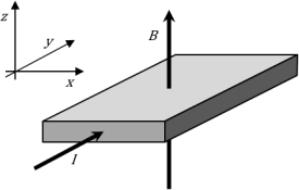
(d) A conventional current of 2.0 mA is passed through a thin strip of an n-type doped semiconductor, 3 mm by 12 mm by 0.5 mm in size, that is held in a magnetic ield, B = 0.5 T. The material is aligned along cartesian axes as illustrated, with the current directed in the +g-direction and the magnetic ield in the +y-direction. A Hall voltage develops and is given by Ⅴ = wRH JB , where w is the sample width, RH is the Hall coefficient, and J is the current density. Estimate the Hall voltage (both magnitude and direction) when the donor dopant density is 1022m-3 . [4]
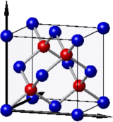
2 (a) Crystalline indium phosphide, InP, adopts an fcc lattice structure with a lattice constant of 587 pm. It has a two-atom basis comprising an In atom at (0, 0, 0) and a P atom at ( 1/4 , 1/4 , 1/4 ), as illustrated. Sketch the arrangement of atoms on the (110) plane that cuts through the conventional unit cell, showing clearly the cell dimensions and the positions of all atoms in the plane. [3]
(b) The structure factor describing difraction is given by Fhkl =:j fjeiGhkl.rj .
i. Define all the terms in this equation. [2]
ii. Determine the structure factor for Inp, showing that it can be written as the multiplication of a lattice term and a basis term. [4]
iii. By considering just the fcc lattice, determine the two sets of Bragg re-lections that are the closest sgstematic absences to the origin of an x-ray difraction pattern collected from Inp. [3]
(c) How, qualitatively, might the difraction pattern of Inp be distinguished from that of elemental Ge, which adopts the same structure as Inp but with a lattice constant of 566 pm and with all atoms replaced by Ge? [3]
(d) InP has a direct band-gap of 1.344 eV. Outline how the optical absorption coefficient could be measured and sketch its predicted variation with optical wavelength. [3]
(e) It can be shown that the carrier density in an intrinsic semiconductor is approximated by the equation:
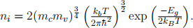
If an Inp sample is doped with tin (sn), an n-type dopant, calculate the sn concentration (in parts per million) required for the extrinsic carrier density to dominate at a temperature of 850 K.
At the k-value of the band gap, conduction electrons have an efective mass of 0.08 me and valence holes have an efective mass of 0.56 me, where me is the rest mass of the electron. [6]
2023-08-07