FEEG2004W1 ELECTRONICS, DRIVES AND CONTROL SEMESTER 1 EXAMINATIONS 2020/21
Hello, dear friend, you can consult us at any time if you have any questions, add WeChat: daixieit
FEEG2004W1
SEMESTER 1 EXAMINATIONS 2020/21
ELECTRONICS, DRIVES AND CONTROL
DURATION - 24 hours
Q1.
Consider a two-degree-of-freedom mechanical system shown in Figure Q1.
(b) Show that the transfer function between the input f(t) and the
output x (t) using Laplace transform is k when 2 s(mcs2 +mks+kc) initial conditions are zero. [7]
(c) Find the time response x2 (t) to a unit impulse input
f(t) = δ(t) using inverse Laplace transform with zero initial conditions when m = 1kg, c = 1Ns/m and k = 4N/m. [7]
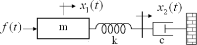
Figure Q1
[Total: 20 marks]
Q2.
Consider the block diagram shown in Figure Q2.
(a) Simplify the block diagram and obtain the closed-loop transfer function R(y)![]()
![]() [6]
[6]
(b) Use the Routh-Hurwitz criterion to find the range of K for which the closed-loop system is stable. [4]
(c) Calculate the natural frequency and the peak time when K = 8. [4]
(d) Sketch the root locus for the open-loop transfer function ![]() when K varies from zero to infinity. [6]
when K varies from zero to infinity. [6]
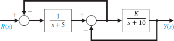
Figure Q2
[Total: 20 marks]
Q3. (a)
An amplifier is required to have a voltage gain of +80dB over the frequency range 0 to 10kHz. Design a suitable circuit employing operational amplifiers (op amps) that have an individual gain bandwidth product (GBP) of 106 . Draw the circuit diagram and indicate suitable values for the resistors used. [4]
Explain briefly the reason why the op amps have a deliberately limited GBP. [2]
Assuming the individual op amps have a slew rate of 10 Volts per microsecond, calculate the maximum peak input voltage of a 10Khz sinewave before the onset of slewing in the output signal. You must fully explain your solution to obtain full marks. [4]
(b)
Draw an ASM chart that describes the operation of a binary coded decimal (BCD) counter that can be switched by an external logic signal (X) between ‘divide by 3’ operation when X = logic 0 and ‘divide by 6’ operation when X = logic 1. [3]
Explain how the counter can be made to output a logic 1 once per cycle. pulse exactly [1]
With the use of Karnaugh maps derive suitable Boolean equations such that the counter can be implemented using D-type flip-flops. You should indicate clearly how your design deals with any unused states. [6]
[Total: 20 marks]
Q4.
(a)
Design an anti-aliasing filter suitable for use with an analogue to digital converter having a sampling rate of 200KHz. Implement your design using two series connected second order Sallen and Key filters to give a relative attenuation at the Nyquist frequency of 80dB compared to the pass band gain. You may assume that suitable damping factors to give a maximally flat response for the two stages of the filter are 1.848 and 0.765 respectively, as would be obtained from typical filter design tables. [8]
Calculate the overall pass band gain of your filter and explain how an additional stage of amplification could be employed to increase it to +20dB. [2]
(b)
Draw the circuit diagram and explain the principle of operation of a 3 input CMOS NOR gate. [5]
Explain how the output stage of the circuit could be modified to make the gate into a 3 input CMOS OR gate. [1]
Explain briefly how the power consumption of CMOS logic circuits is related to their operating frequency. [2]
Explain briefly why the inputs of some CMOS devices require protection from static electricity and describe how their input circuits can be modified to achieve this protection. [2]
[Total: 20 marks]
Q5.
(a)
With the aid of a suitable diagram show how a single chip microprocessor might be combined with an 8 bit digital to analogue converter (DAC) and an operational amplifier (op amp) comparator to realise a tracking (or servo) analogue to digital converter (ADC). You should clearly indicate on your diagram where the digital output from the ADC is taken.
Clearly indicate your choice of power supplies for the DAC and op amp, assuming that the ADC is required to convert voltages in the range zero to 1V and the single chip microprocessor recognises logic 1 as +5V and logic 0 as 0V. [6]
Using any suitable pseudo programming language (e.g. plain language), write a pseudo code listing to implement the tracking ADC algorithm on the microprocessor used in your design. You may assume the microprocessor has digital inputs and outputs that can be read and written directly by software commands. [4]
(b)
An airport luggage conveyor drive system uses a 3 phase, 2 pole, 60Hz induction motor.
i) If the drive operates at a value of 4% slip (0.04) then calculate the actual rotor running speed. [2]
ii) What frequency of voltage is induced in the rotor of this induction motor at this operating point? [2]
(c)
i) Draw a simple electrical schematic diagram of a single phase H bridge inverter with load, and briefly describe how it can synthesise different pseudo-AC outputs across the load. [3]
ii) For a full three phase variable speed induction motor drive e.g. as used on an electric train, briefly explain and illustrate how such a drive utilises and controls regenerative braking as part of the overall drive control system. [4]
(d)
State what power electronic switch type is illustrated in Figure 5c, briefly describe how this device is turned on and off, and what the role of the integral diode is for. [2]
2023-08-05