Microwave Engineering and RF Circuits, ES3E6
Hello, dear friend, you can consult us at any time if you have any questions, add WeChat: daixieit
Module title and code: Microwave Engineering and RF Circuits, ES3E6
Assessment setter (module tutor): Dr Ryan Montague
Assignment Weighting and typical hours work: Assignment 30% of module. .
Learning outcomes assessed:
• Design of matched RF amplifier circuits.
Requirements/Task: Complete all parts and present them in your assignment report – PDF FILE ONLY.
Assessment criteria/mark scheme: Marking is out of 100% . Marks will be allocated based on the accuracy of your simulations and justification of comments made.
Submission date/deadline: 29th August 2023 via tabula. All submissions that miss this deadline will be subject to the normal 5 marks per day penalty, starting at 12:01 29th August 2023.
SUBMISSION MUST BE IN PDF FILE FORMAT
Additional Useful Resources: AWR videos available on Moodle, content of current and previously covered modules, further video information available on the internet.
Feedback format: Your submitted report will be marked electronically. The marks of the various sections will be provided as well as an outline of the answers of the various sections in order to identify where/how to improve.
ES3E6 Microwave Engineering and RF Circuits Assignment - REFERRAL September 2023
RF Amplifier Design Assignment - Microwave Office (AWR DE)
The aim of this assignment is to design a radio frequency (RF) amplifier based on an Infineon BFR181W low noise,
high gain broadband NPN silicon RF transistor. The circuit topology to be used is a standard four-resistor biased
common-emitter and the principal design goal is to achieve maximum power transfer with matched input and output impedances. The bias point details for the circuit and centre-frequency for design optimization are given in Table 1
below.

Part 1 [8 Marks] - Transistor BFR181W s-parameters
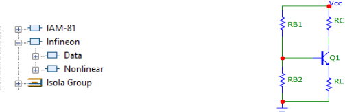
Set up a simulation in Microwave Office using the AWR Elements tab, Libraries, Parts by Vendor library, selecting transistor BFR181W from “Data” folder.

Select the BFR181W transistor from “Low Noise Si transistors up to 2.5 GHz”. Devices within the “Data” folder are linearized, small-signal models with pre-defined collector current and collector-emitter voltage; in effect these models are pre-biased. Select the requisite bias point (Table 1) using the drop-down option boxes for Vce and Ic (double-click the current or voltage value as appropriate). To design the required RF amplifier, you must first determine the transistor’sS-parameters at the required frequency of operation (centre-frequency). Set-up a single frequency analysis at the centre-frequency and add “New Graph” type “tabular”, adding measurements for all S-parameters. This is simple to do in AWR by using “ports” at the input and output as shown below.

Determine the s-parameters in rectangular form for centre-frequency, characteristic impedance and given bias point.
Part 2 [40 Marks] - Design for optimum gain
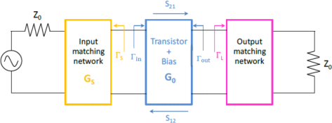
To obtain maximum available gain from your amplifier you must match both the source and load impedance to the input and output ports of the transistor. To achieve this, you must design matching networks for both the input and the output, as shown in the figure below.
(MATLAB) Design equations: determine the input reflection coefficient (ΓS ) and output reflection coefficient (ΓL ) as follows:
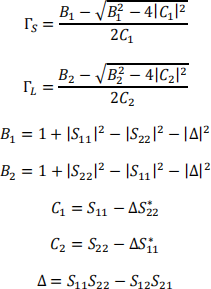
(Note the design equations above ensure that the amplifier is simultaneously conjugate matched for both the input and output reflection coefficients.)
Having determined input reflection coefficient (ΓS ) and output reflection coefficient (ΓL ), calculate the required
values of source and load impedance the input and output matching networks must present in order for maximum power to be transferred from input to output.
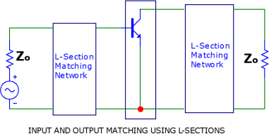
Simultaneous Conjugate matching networks: there are many potential matching networks that can be used for this design problem. However, for this design you are required to use lumped component L-section passive LC matching as indicated in the figure below.
Once you have determined the values of L & C for each section (there are dozens of LC matching network calculators available online), create a new schematic to include the input and output matching networks. Simulate over the
frequency range 300MHz ≤ f ≤ 900MHz and produce the following:
1. Rectangular plots of the magnitudes of S11 and S22 in decibels (dB) vs logarithmic frequency. Explain how the plots of S11 and S22 vs frequency plots demonstrate that you have correctly simultaneously conjugate matched both the
input and output of the overall amplifier.
2. Rectangular plots of the magnitudes of S21 and S12 in decibels over logarithmic frequency scale.
Evaluate the overall performance of the amplifier by comparing the measured gain at the centre-frequency with the theoretical optimum gain given by,

Part 3 [40 Marks] - Bias network and nonlinear modelling
For this section use the full non-biased, nonlinear model of the transistor BFR181W which can be found in the
“Nonlinear” folder. Now design a four-resistor bias circuit (as shown below) to locate the transistor at the same bias point as given in Table 1. The design must adhere tobias stability rules and normal rules of thumb for BJT-based amplifiers. Provide details of all calculations used to determine the bias components.
Using the IV curve tracer (element IVCURVEI![]() ) plot the IV characteristics of the BFR181W and estimate a
) plot the IV characteristics of the BFR181W and estimate a
value for the forward current gain β at the bias point given Table 1. Plot typical IC vs VCE curves that include the
required bias point from which you can estimate β. Calculate the required bias components, RB1, RB2, RC and RE
based on the typical rule of thumb that 10% of VCC is dropped across the emitter resistor and the collector voltage is set for maximum ac swing. The Thevenin impedance of the base bias chain should be equal to 0.1RE × β. Simulate the amplifier circuit with the calculated values and demonstrate that the required Q-point has been achieved.
Part 4 [12 Marks] - Linear versus nonlinear modelling
Now connect the input and output matching networks andre-assess how well the overall amplifier is matched by
comparing the magnitude (dB) plots of S11 and S22 both with and without the four-resistor bias network. Comment on your findings.
2023-07-26