ES4E8 Advanced Power Electronic Converters and Devices Laboratory 2
Hello, dear friend, you can consult us at any time if you have any questions, add WeChat: daixieit
ES4E8 Advanced Power Electronic Converters and Devices Laboratory 2
Module title and code: Advanced Power Electronic Converters and Devices, ES4E8
Assessment setter (module tutor): Dr Oleh Kiselychnyk
Assignment Weighting and typical hours work: The assignment is assessed only through questions in the QMP exam test. 4-6 hours including the lab session.
List the LO’s being assessed: Understand the operation and conceptual design principles of advanced power converters with PWM control.
Context/Introduction/Background to the assignment: The lab instructions are provided below.
Requirements/Task: No report is required but it is recommended to fill in the proforma which you can
use during the QMP exam. Please answer all questions in the attached proforma (the bold questions in the laboratory instructions).
Formatting requirements: No requirements.
Submission date/deadline: No deadline.
Assessment criteria/mark scheme: The assignment is assessed only through questions in the QMP exam test.
Feedback format: Answering questions during the lab session and while filling in the proforma.
ES4E8 LABORATORY 2 BRIEFING SHEET
NOTE: please ensure that you bring along a memory stick to the laboratory session, for saving your waveforms and oscilloscope screen shots. Alternatively, you may use your phone to make photos of the screen shots.
The goal of the laboratory is to learn experimentally the operation principle of a three-phase frequency converter with sinusoidal PWM generation.
1. THEORETICAL BACKGROUND
The electrical schematic of a three-phase inverter supplying a three-phase symmetrical resistive load is depicted in Fig. 1.
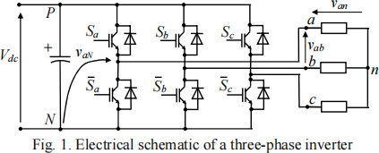
The inverter converts an input DC voltage Vdc into a three-phase symmetrical AC voltage applied to the load. It consists of three legs (a, b and c) and each leg includes two switches implemented based on IGBT transistors with anti-parallel diodes. Sa , Sb and Sc denote the corresponding gate control logical signals of the top transistors of the legs. If Sa = 1 then the corresponding top transistor is open or on (can conduct the current in the direction shown by the transistor arrow). Otherwise Sa = 0 and this transistor is closed or off (cannot conduct the current). Similar applies to the top transistors in legs b and c. The gate control signals of the bottom transistors are complementary signals of the gate control signals of the top transistors as shown in Fig. 1. P and N denote positive and negative bus bars of the DC link.
If Sa = 1 then the pole voltage of leg a is VaN = Sa Vdc = Vdc . If Sa = 0 then VaN = Sa Vdc = 0 . The similar is in the legs b and c. Since there are three independent control signals then eight switching combinations are possible for the inverter with the pole voltages summarized in Table 1.

The line-to-line inverter output voltages are found as vab = vaN 一vbN , vbc = vbN 一vcN and vca = vcN 一vaN .
The phase load voltages are computed based on the line-to-line voltages and the condition of the balanced
load van +vbn +vcn = 0 . For example, vab = van 一vbn = van + (van +vcn ) = 2van +vcn . Then van = ![]() vab 一vcn ) . Note that vcn = vca +van . Then vcn = vca +
vab 一vcn ) . Note that vcn = vca +van . Then vcn = vca + ![]() vab 一vcn ) and vcn =
vab 一vcn ) and vcn = ![]() 2vca +vab ). The phase voltages van and
2vca +vab ). The phase voltages van and
vbn are found similarly.
The sinusoidal PWM modulation of the gate control signals is realised according to Fig. 2.
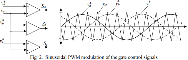
For each leg of the inverter there is a sinusoidal reference voltage vi(*) . The references vb(*) and vc(*) are shifted with respect to the reference va(*) by 120 and 240 electrical degrees, respectively. These references are at all times compared with a high-frequency triangular carrier signal vcr . If vi(*) > vcr then Si = 1 else Si = 0 .
The pole voltage of leg a, the line-to-line voltage between points a and b, and the phase voltage in phase a of the load obtained based on the control from Fig. 2 are presented in Fig. 3.

Note that the frequency of all voltages in Fig. 3 is equal to the frequency of the reference voltages. The amplitudes of the fundamental components of the voltages are proportional to the amplitude of the reference voltages.
The pole voltage can only have two levels 0 V and Vdc . The fundmental components of the pole voltages have a DC offset equal to Vdc / 2 . Note that the thickest positive pulse of the pole voltage (corresponds to the thickest gate control pulse for the corresponding top transistor) is at the maximum of the corresponding reference voltage. The sickest zero pulse of the pole voltage is for the minimum of the corresponding reference voltage. The duty ratio for the corresponding top switch will be the ratio of the fundamental component and Vdc value. If the fundamental component of the pole voltages has amplitude Vdc / 2 then the maximum duty ratio is 1 and the minimum duty ratio is 0. For an arbitrary amplitude of the fundamental component Vmfc < Vdc / 2 the maximum duty ratio is (Vmfc +Vdc / 2)/ Vdc = Vmfc / Vdc +1/ 2
and the minimum duty ratio is (Vdc / 2 一 Vmfc )/ Vdc = 1 / 2 一Vmfc / Vdc . In general, the duty ratio of the top
transistor in each leg is a function of the corresponding leg reference signal di = vi(*) / 2 +1/ 2 for the case if
vi(*) < 1 and the amplitude of the carrier is equal to 1.
The line-to-line output voltage has no DC offset and it has three voltage levels 0 V and 土Vdc . The thickest positive and negative voltage pulses are at the maximum and minimum of the differences of the
corresponding sinusoidal reference signals (in case of Fig. 3 it is va(*) 一vb(*) ). The thinnest pulses are when the voltage va(*) 一vb(*) crosses the time axis.
The phase load voltage has five levels 0 V, 土Vdc / 3 and 土2Vdc / 3 .
The amplitude modulation index of the inverter is determined as the ratio of the amplitude of the reference voltages and the amplitude of the carrier ma = Vi m(*) / Vcrm . The frequency modulation index is the ratio of the frequencies of the carrier and the reference voltages mf = fcr / fvi(*) .
2. EXPERIMENTAL RIG
The experimental rig includes the following main components:
. A three phase frequency converter
. An isolating single-phase transformer separating the converter from the mains
. A single-phase autotransformer (variac) allowing to regulate the amplitude of the AC voltage supplied to the converter
The electrical schematic of the frequency converter is presented in Fig. 4. It consists of an uncontrolled diode rectifier, a DC link with capacitors and an inverter. There is additionally a DC chopper. The converter is in a transparent plastic box. There is no internal connection between the output of the rectifier and the DC link of the inverter. The logical gate control signals (with 0/15 V level logics) are supplied to the gates of the corresponding transistors via gate drivers providing necessary voltage level shift sufficient for transistor switching on/off and galvanic isolation of the converter with external control circuits. In
Fig. 4 four external connectors R, Y, B and Bk mean red, yellow blue and black, respectively. These colours denote the recommended colours of wires to be connected to these connectors. Ti, Bi and Chop denote inputs for logical gate control signals. All power circuit connectors are on the top of the converter box as shown in Fig. 5. The connectors for the control signals and the DC chopper current and voltage measurements are on the front side of the box. The Error connectors are used for protection and communication with a control unit of the inverter. If there is a fault the control system must disable the inverter. There are also connectors for connection of an external +15V DC supply for feeding the gate drivers.

The test rig also includes the inverter control unit. It is programmable, multi-function PWM controller. For this laboratory, only one operating mode of the controller will be used.
It is three-phase induction motor V/f=const speed controller. It allows to generate gate control signals which provide a constant ratio of the fundamental component magnitude of the inverter output phase (and line-to-line) voltage and the frequency of this voltage. This assures that the mechanical characteristics of the induction motor are with a constant critical torque for the whole speed regulation range. For different frequencies the characteristics have almost the same stiffness.
The top view of the control unit is depicted in Fig. 6. You can switch power on/off and reset the control unit from the back side.
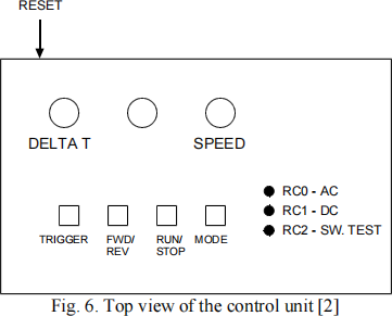
The modes are selected using the “Mode” button on the controller. Each time this is pressed, it cycles between three modes: AC, DC and switching test. The DC mode is inactive here and is not used during the tests. There are three coloured LEDs in the unit indicating the active mode:
|
RC0: Red: |
AC |
|
RC1: Yellow: |
DC is not used |
|
RC2: Green: |
Switching test is not used in this lab |
AC Mode
There are two buttons used in this mode: Run/Stop and Fwd/Rev. The buttons perform the following
functions:
Run/Stop: Starts and stops the motor (gate control signals Ti and Bi).
Fwd/Rev: Changes the direction of the motor rotation (changes the sequence of the gate control pulses).
The control knob marked “speed” controls the speed (the frequency of the generated voltages). The amplitudes (and rms values) of the fundamental components of the voltages (both phase and line-to-line output voltages) change proportionally to the frequency. The frequency varies from 5 Hz to 50 Hz.
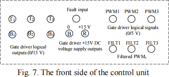
The front side of the control unit gives an access to the generated gate control signals with 0/15 V logics (Ti and Bi), to the 0/5 V logics gate control signals (PWMi) and to the filtered 0/5 logics signals (FILTi) as shown in Fig. 7. There are also outputs for supplying +15 V DC voltage to the inverter drivers and a Fault input which is connected to all Error outputs of the inverter.
The additional equipment associated with the laboratory is:
. 4-channel oscilloscope
. Two differential voltage probes
. One current probe (clamp)
. 3-phase induction motor
. 2 digital voltmeters (DVM)
The key tasks will be to observe:
. PWM switching waveforms from the inverter control unit
. Simple V/f=const control of the induction motor
. Rectifier voltage waveforms
. Inverter pole and line-to-line voltages waveforms
3. INITIAL SETUP
The isolating single-phase transformer will be already connected to the mains. Make sure that the single- phase autotransformer (variac) is switched off. Connect the autotransformer (variac) to the isolating transformer plugging it in. The single-phase output of the autotransformer on its top should be connected to any two input phases of the converter rectifier. Connectors R and Bk in Figs. 4 and 5 are recommended. Connect one digital voltmeter (DVM) to the rectifier DC outputs (set to 600 VDC setting or auto) and another DVM between two input phases of the rectifier connected to the autotransformer (set to 750 VAC setting). Make sure these voltmeters are turned on and visible all the time.
Turn on the single-phase supply on the back of the control unit. The PWM starts in no-mode operation (all 3 LEDs on).
Saving the Oscilloscope Data
The oscilloscope images may be saved on to a memory stick as png files. First insert a memory stick into the socket in the lower bulkhead MDO3024. Press the SAVE button on the scope when you need to save a screen shot.
The points in the laboratory at which screen shots of waveform data must be saved are indicated in bold. Measurements that must be taken and points that must be discussed in the write-up are also given in bold. You do not need to carry out the calculations until after you have finished the laboratory.
|
IMPORTANT:
The autotransformer (variac) should always be turned to ZERO VOLTAGE whenever changing connections on the rig. Please do not use the on/off switch for this purpose. Switch off the autotransformer (variac) only after you have completed the laboratory or in case of emergency. |
4. RECTIFIER OPERATION
The first task is to test the operation of the single-phase diode rectifier. Note that the rectifier has input three phases. However, only two of them are connected to AC voltage. The third one is left unconnected. This connection is equivalent to a single-phase diode bridge rectifier.
Make sure the rectifier is not connected to the inverter, and that the connections in section 3 are made. Also connect one differential probe to the rectifier input (R, Bk phases) and channel 2 of the scope as shown in Fig. 8. Connect the other differential probe to the rectifier output and channel 1 of the scope.
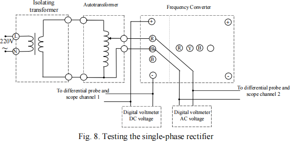
Set both differential probes to x200. Set the scope to 4 ms/div (use the Horizontal scale of the scope, channels 1 and 2 should be on), and trigger (use Trigger menu of the scope following by the menu at the bottom of the screen) from channel 1 (DC coupling, auto trigger, rising edge). Set both channel 1 and 2 to probe attenuation of x20 (press channel number button of the scope following by the pressing button “More”. Choose Probe setup and set the attenuation using the knob a with the circle). Note this will give a x10 factor on the trace. Set both channels to 10V/div using the knobs of the corresponding scope channels (i.e. with the factor of 10 this gives and effective 100V/div).
Turn the autotransformer (variac) on. Slowly increase the autotransformer (variac) output voltage to 230 V. Check the voltage value using the DVM connected to the rectifier input. Observe the waveforms displayed on the screen. Take a scope screen shot (you may need to hit “run/stop” or “single” buttons on the scope to get a stationary waveform. You may need to adjust the trigger level).
You may use scope cursors to determine the difference between two horizontal or vertical levels of the scope signals. Press button “Cursors” of the scope and hold it for a while. There appears a menu at the bottom of the screen where you can choose between horizontal (time) and vertical (voltage level) cursors. After selecting necessary cursors you can move two cursors on the screen using knobs a and b with the circles. The difference between the cursor positions is shown in the rectangle at the top of the screen. For horizontal cursors the difference is shown as real time difference. For vertical cursors it already includes the channel attenuation. For example, if channel attenuation is x20 and differential probe attenuation is x200 then actual measured 300 V will be shown as cursor difference 30 V. So the cursor difference must be multiplied by the attenuation of the probe and divided by the attenuation of the scope channels to obtain the actual value.
At 230 V, measure:
. The AC input rectifier voltage (rms and amplitude) – use the AC voltmeter reading and the scope
. The peak voltage from the rectifier and the voltage ripple using the scope
. The average DC voltage of the rectifier output – use the DVM
Turn the autotransformer (variac) back to 0 V. Take the differential probes out, but leave the DVMs connected.
5. PWM SWITCHING WAVEFORMS
The second task is to observe the PWM switching waveforms.
PWM logic signals
Press the MODE button on the PWM controller until the red LED (AC mode) comes on. Press the RUN/STOP button on the controller. Connect the PWM1 output from the controller into channel 1 on the scope. This measures the raw digital logic gate control signal (0/5V) coming from the controller. Set channel 1 to x1 attenuation, 2V/div, 20μs/div (you may need to hit “run/stop” or “single” buttons on the scope to get a stationary waveform. You may need to adjust the trigger level).
Observe what happens as you vary the SPEED control on the controller.
Set the maximum speed and take a scope screen shot.
. Measure the period of the square wave
. Calculate the switching frequency
. Measure the times on and off for one period in the screen shot
. Calculate the duty ratio of the signal for one switching period in the screen shot
. Take one more screen shot after hitting the run/stop button of the scope. Are the times on and off the same? Explain the reason.
Remove any leads from PWM1, PWM2 or PWM3.
PWM gate drive signals
Now you will measure the gate control waveforms coming from the controller to the inverter. In the inverter, these are passed through an isolating stage to drive the actual IGBT gates. The inverter requires 0/15V logic signals, generated from the 0/5V logic using a level shifter. Here you will measure the 0/15V gate signals.
Connect the outputs T1 and B1 into scope channels 1 and 2, respectively. Set both&
2023-07-19