ES4E8 Advanced Power Electronic Converters and Devices Laboratory 1
Hello, dear friend, you can consult us at any time if you have any questions, add WeChat: daixieit
ES4E8 Advanced Power Electronic Converters and Devices Laboratory 1
Module title and code: Advanced Power Electronic Converters and Devices, ES4E8A1 Laboratory Assignment 1
Assignment setter: Dr Marina Antoniou
Assignment Weighting and typical hours work: 30% of module. Typical hours of work: 45 hours.
Learning outcomes assessed:
• Apply advanced concepts through the use of device physics in the context of device design.
Context/Introduction/Background to the assignment: Based on material of the module and instructions provided below.
Formatting Requirements: Typed answers expected. Minimum font (times roman) size: 12 pt. Handwritten answers (provided they are legible) can be scanned and submitted, or a combination of typed and scanned handwritten work. Insert screen-shot pictures in your answers where appropriate.
Submission date/deadline: 12 noon Thursday 23rd Feb 2023.
Requirements/Task: In this assignment there are THREE questions. Please answer all questions.
Assessment criteria/mark scheme: The marks percentage for each part is shown in the square brackets. Marking is out of 100%.
Feedback format: Your submitted report will be marked electronically. The marks of the various sections will be provided as well as an outline of the answers of the various sections in order to identify where/how to improve.
Question A
A= (last two digits of your university ID number+250)
B= (last two digits of your university ID number×9+800)
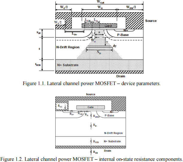
1. Figure 1.1 shows the basic cell structure of a power MOSFET.
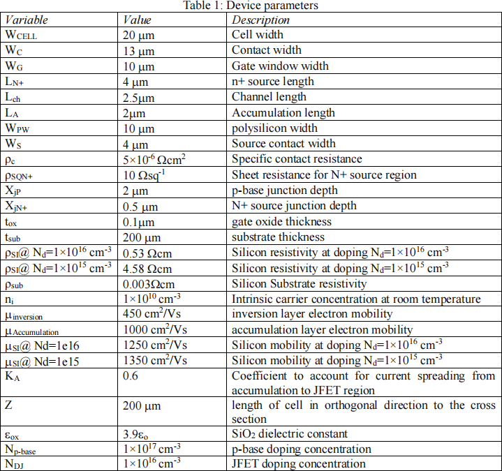
Describe the internal resistance components in the power MOSFET on-state operation as shown in figure 1.2 and comment on their effect as the device voltage rating increases. [5%]
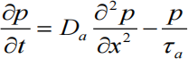
2. Calculate the on-state resistance % contribution of each internal resistance component over the total on-state resistance for a “A”V breakdown rated MOSFET @ Vgate=15V, Vthreshold= 7V and Vdrain=0.5V (where the value of “A” is defined above). Identify the most important resistance
contributions.
Use the device parameters as given in table 1 (you may find reference [1], section 6.4 & 6.5 useful for this analysis). [10%]
3. Calculate the on-state resistance % contribution of each internal resistance component over the total on-state resistance for a “B”V breakdown rated MOSFET @ Vgate=15V, Vthreshold= 7V and Vdrain=0.5V (where the value of “B” is defined above). Identify the most important resistance
contributions and discuss how these compare to your finding in part (2).
Use the device parameters as given in table 1 (you may find reference [1], section 6.4 & 6.5 useful for this analysis). [5%]
4. Using MATLAB (or analogous software) discuss how the variation of Gate electrode width Wg affects the performance of the device in part (3) with specific reference to internal resistance components. The cell width should remain constant. Illustrate your answers by means of corresponding plots. [5%]
5. Discuss how a “B”V breakdown rated IGBT structure on-state resistance contributions might change. Assume that the Device parameters remain the same, except for the substrate; now this layer is ann-buffer layer and p+ anode layer (where the value of “B” is defined above). [5%]
6. Discuss how a “B” V breakdown rated Silicon Carbide MOSFET device would alter the on-state resistance contributions (where the value of “B” is defined above). [5%]
References
[1] Book “Fundamental of Power semiconductor Devices” B.J. Baliga, Springer International Publishing 2008.
Question B
Ambipolar Conduction (aka Conductivity Modulation)
Conductivity modulation is the charge compensation effect that occurs under high level carrier injection. High level is defined by the rule of thumb that in injection level is > 10% of the background doping level. Both carrier species are equal, this allows the basic transport equations to be modified to produce ambipolar transport. Very low resistance bipolar power devices such as diodes, thyristor and IGBTs use this effect to reduce the on state resistance. Charge is removed slowly by diffusion and recombination controlled by ambipolar diffusion equation.

Figure 2.1: PiN diode On-state Carrier Density Distribution
The idea here is that under such high-level injection conditions, the two equations for electron and hole continuity can be combined into a single equation. This means we only need to solve one equation instead of two. To do this we make the assumption that, we only need solve for on carrier density since:
p(x) = n(x)
where
Which has the general solution:

Where A and B can be found from the appropriate boundary conditions.
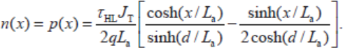
Where d is distance from the middle of the device (fig. 2.1) and JT is the current density
where

Figure 2.2: Simulated silicon PIN Diode
Drift Length = DL= (last two digits of your university ID number×4+100) μm
Current Density JT=50A/cm2
Lifetimes: τ = 1, 3, 10μsec
Mobility of Electrons at T=300°K
μe=1417 cm^2/(Vs);
Mobility of Holes at T=300°K
μp=471cm^2/(Vs) ;
1. Explain what the difference between bipolar and unipolar devices is. How do we decide which device to use for a specific application? [5%]
Given the theory above,
2. Use the analytical equations above to calculate and plot using MATLAB (or analogous software) the charge concentration across the PIN Diode structure (figure 2.2) for all three ambipolar lifetimes values at room temperature. [10%]
3. Use the analytical equations above to calculate and plot using MATLAB (or analogous software) the charge concentration across the PIN Diode structure (figure 2.2) for an ambipolar lifetime = 1μs at 65° and 125°C. [10%]
4. Use the analytical equations above to calculate and plot using MATLAB (or analogous software) the charge concentration across the PIN Diode structure (figure 2.2) and drift length 2*DL (where DL is defined above) for an ambipolar lifetime=5μs at 125° C. How do the two drift region lengths charge concentration distributions compare? How will this device performance change under the on-state and breakdown conditions? [5%].
Question C
Figure 3.1 shows the on-state characteristics of a 3.3kV Silicon and Silicon Carbide PIN diodes at 25°C.
The blocking Silicon p-n junction consists of ap-type region containing 1019 cm-3 acceptors (NA) and an n-type region containing of 1014 cm-3 donors (ND). The intrinsic carrier concentration at 300K (25°C) is 1.01 × 1010 cm-3. Assume that VT, the thermal voltage, (=kB*T/e, where T is the absolute temperature, kB is the Boltzman constant and e is the charge on an electron) is 26mV at room temperature.
The blocking SiC p-n junction consists of ap-type region containing 1019 cm-3 acceptors (NA) and an n-type region containing also of 1015 cm-3 donors (ND). The intrinsic carrier concentration at 300K (25°C) is 5×10⁻⁹ cm-3.
1. Justify the shape of the two curves given the material properties (i.e. Vo value and differential resistance (line curvature))? (15%)
2. Discuss which material you would use for applications of 15A/mm2. (10%)
3. Discuss why SiC Schottky diodes are preferable for high current applications (>20A/mm2). (10%)
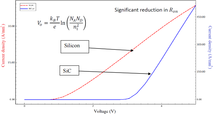
Figure 3.1: The on-state characteristics of a 3.3kV Silicon and Silicon Carbide PIN diodes at 25°C
2023-07-19