Electrical Circuits and Devices (ELCD)
Hello, dear friend, you can consult us at any time if you have any questions, add WeChat: daixieit
Experiments Instructions Sheet
Characterisation of Op-Amp Circuits
Electrical Circuits and Devices (ELCD)
International Year One in Engineering
1. Introduction
This is software and hardware experiments exercise forms one of your assessed submissions and will be used to assess your practical and theoretical progress in this module. It will also assess your theoretical and practical skills in addition to your technical report writing skills. The report is weighted 20% of your total grade of this module.
2. Experiment Brief
This report is based on the work you do to study the performance of some typical op-amp circuits using Multisim software tool and/or advanced solderless breadboard. In particular, you are instructed to build and analyse a comparator, follower, non-inverting amplifier, inverting amplifier, differentiator, and integrator using software and hardware and comment on the results.
3. Software Tool
You will need to use the Multisim software tool to complete these experiments. There are some options for you to access this software, check the Technical Requirements section on the Module Information page of the ELCD Canvas site.
4. Procedure
Connect the following circuits:
a. Comparator (Figure 1)
Apply a 1 kHz sine wave signal of about 1 Vp−p to the noninverting + input, with the inverting − input grounded. Observe this signal on the oscilloscope, triggering on external. Plot the output signal against the input signal. Does it change if you reduce the input voltage to 0.1 V? What is the effect of grounding the + input and connecting the signal to the − input?
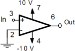
Figure 1: Comparator circuit
b. Follower (Figure 2)
Apply the same signal to the input as in Part a . Note that with negative feedback (to the inverting input) the op-amp adjusts its output so that the inverting input is at the same voltage as the noninverting input. What is the signal at the output? Plot it against the input signal. What is the input impedance of the circuit? What happens with a square wave input?
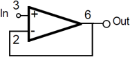
Figure 2: Follower circuit
c. Non Inverting Amplifier (Figure 3)
The two 1 k![]() resistors divide the signal at the output of the amplifier by a factor of two. In order for the voltages at the two inputs to the amplifier to be equal the circuit must have a gain of two. Apply the same signal as in Part a to the input. What is the signal at the output? Plot the output signal against the input signal. What is the signal at the inverting input? What is the gain of the amplifier? What happens when the input voltage is too large? What happens with a square wave input? How would you change the circuit to make the gain equal to 10?
resistors divide the signal at the output of the amplifier by a factor of two. In order for the voltages at the two inputs to the amplifier to be equal the circuit must have a gain of two. Apply the same signal as in Part a to the input. What is the signal at the output? Plot the output signal against the input signal. What is the signal at the inverting input? What is the gain of the amplifier? What happens when the input voltage is too large? What happens with a square wave input? How would you change the circuit to make the gain equal to 10?
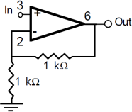
Figure 3: Non inverting amplifier circuit
d. Inverting Amplifier (Figure 4)
In this circuit the noninverting input is at ground. In order to keep the inverting input near ground the amplifier must "balance" a positive input with a negative output, and vice versa. Measure the voltage at the inverting input. The inverting input is said to be at a "virtual ground." Observe the performance of the amplifier on the oscilloscope. What is the gain of the amplifier? Plot the output signal against the input signal. What happens if you connect the inverting input to a “real” ground? The input impedance of a circuit is the ratio of the input voltage to the input current. With a 1 V input, calculate the current flowing through the 1 k![]() input resistor. What is the input impedance of the circuit? How would you change the circuit to make the gain equal to −10?
input resistor. What is the input impedance of the circuit? How would you change the circuit to make the gain equal to −10?
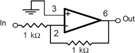
Figure 4: Inverting amplifier circuit
e. Differentiator (Figure 5)
This circuit differentiates the input voltage. Since the inverting input is at a virtual ground, the current flowing through the 1 kQ resistor, and hence the output voltage, is proportional to the derivative of the voltage across the 0.2 uF capacitor.

Apply the same signal as in Part a to the input. What is the signal at the output? What is the output with a triangular wave input? Plot the output signal against the input signal.
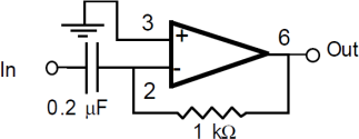
Figure 5: Differentiator circuit
f. Integrator (Figure 6)
In this circuit the capacitor and the resistor are interchanged and the signal is integrated instead of differentiated. In addition, a 100 kQ resistor has been added to prevent any input offset voltage that might be present from driving the output of the op-amp to one of its extreme limits. Apply the same signal as in Part a to the input. What is the signal at the output? What is the output with a square wave input? Plot the output signal against the input signal.
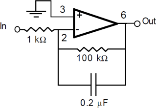
Figure 6: Integrator circuit
Assignment Submission
The report should be Word processed, on A4 paper size. Your written report must be submitted to the Canvas site of the module by the specified deadline on Canvas.
5. Report Length and Contents
The word limit for the report is 2,000 words (±10%), excluding figure and table captions, equations and reference list. Write the word count on the title page. The report must include:
Title page – with module name, report title, candidate number and word count.
Contents list – with page numbers to include introduction, circuit types, testing, error source, applications, conclusions and reference list.
Results of measurements – with answer to each question, explanations of what you did and why.
Circuits Characterisation - analysis of results. You should support your report with your circuit diagram and circuit response plots using Multisim software tool and/or practically using advanced solderless breadboard and oscilloscope.
Conclusions – containing no new material but summarising what has been achieved.
Reference list – numbered source details corresponding to the cross-reference numbers in the report.
6. Assessment Criteria
The following criteria apply:
Mark Range Criteria
80-100 An exceptionally well written and presented report which covers all of the criteria below and is indicative of individual initiative and originality.
70-79 A very well written and presented report, which covers all of the aspects below and also discusses the background and objectives of the experiments and shows good understanding of building, testing and analysing op-amp circuits.
60-69 A well written and presented report which covers all of the aspects below. In addition, the candidate presents the source errors with explanation.
50-59 A complete record of the test undertaken with an evaluation of the outcomes. The account demonstrates that circuits were correctly built and specified according to the experiments instructions sheet, that it could be constructed, that the circuit was tested correctly and that its performance was appropriately analysed.
40-49 A clear record of the test undertaken and an evaluation of the outcomes. The account demonstrates that circuits were built according to the experiments instructions sheet, although there may be some errors in simulating the circuits, that it could be constructed and that the circuit was tested appropriately.
30-39 An adequate record of the test undertaken. The account demonstrates that the circuits were built according to the experiments instructions sheet and that some progress was made towards testing the circuit.
0-29 There will have been no submission or a seriously inadequate report which indicate that the experiment objectives were not addressed.
2023-06-17
Characterisation of Op-Amp Circuits