CSE140L Lab 4
Hello, dear friend, you can consult us at any time if you have any questions, add WeChat: daixieit
CSE140L Lab 4
1. Objective: Design an encrypter which reads a message from a range of locations in a register file (memory) in 8-bit ASCII format, encrypts the lower 6 bits with a 6-bit PN code, and writes the resulting encrypted message into another range of locations in the same register file.
(In Lab 5, we shall decrypt a given encrypted message.)
2. Deliverables:
2.1 Working Verilog model, built around a state machine for control/sequencing and a simple data path.
2.2 Screenshots of waveform viewer and transcript, demonstrating that it worked properly.
2.3 Screenshot of Quartus RTL Viewer, showing top level block diagram / schematic of your design.
3. Provided:
3.1 Verilog test bench
3.2 Shells for top level Verilog module, register file (data memory)
4. Details of required functionality:
4.1 The testbench will store a given 8-bit ASCII character string (which you or the TAs can easily change) as the original unencrypted (bare) message into addresses 1 through N, where N<52 of a 128-element 8-bit-wide register file (data memory) you will design as a module within your encrypter. The test bench will also put an ASCII underscore (0x5F) into data_mem address 0. This will be helpful to you when you encrypt the preamble.
4.2 Your encrypter/encoder will prepend this message with a prefix comprising at least 7 bytes of ASCII underscore = 0x5F. The test bench will load the desired prefix length into address 61 of your register file and automatically limit the prefix length to 7 to 12 characters. Again, for your convenience, the test bench preloads 0x5F into data_mem[0].
4.3 The test bench will append enough ASCII underscore (0x5F) characters to the end of your message to pad the total length of prefix plus message to 64 bytes.
4.4 Your encoder will bitwise XOR the lower 6 bits of the first 0x5F (ASCII 8-bit underscore) against the given 6-bit LFSR starting state, which the testbench will have stored in register memory location 63. Write this new byte into memory location 64.
1) read LFSR starting state (2 “0” bits followed by 6 LFSR starting bits) from data_mem[63] and load into a register I called “start” (see starter code lines 19, 22, 93);
2) read from data_memory with raddr = 0;
3) set data_mem data_in = data_out ^ {2’b0,start}, waddr = 64, write_en = 1;
You have just encrypted the first character of the preamble, 0x5F with the starting state of the LFSR – that is you first output bit
4.5 For the next pre_len – 1 clock cycles, continue to read from data_mem raddr = 0, continue to advance the LFSR each time, and write the encrypted underscore character into waddr 65, 66, … , up to waddr = 64 + pre_len – 1.
4.6 Now bitwise XOR each succeeding byte of the raw message with each new state of the LFSR, for the LFSR feedback bit pattern the testbench has stored in register memory location 62. Write each successive byte of the encrypted message into locations 63+pre_len, 64+pre_len, ... , 127.
4.7 Compare your results against those given by the testbench.
4.8 Your design must be buildable/synthesizable. In particular, this means you will have to generate address pointers to read from and write to the data memory and data bus connections into and out of the data memory. You are not allowed to “drill down” inside, as I do from the test bench or in my demo design. Think about how the data path is built in a typical RISC (ARM, MIPS, SPARC, etc.) processor.
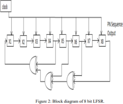
Sample 8-tap LFSR (see Powerpoint for a 6-tap example)
If we number the bits X0 through X7 instead of the X1 through X8 shown, we can express the feedback pattern as:
X7, X5, X4, X3 = binary 1011_1000 = 0xB8.
Your 6-tap LFSR should be able to work with any combination of feedback taps (the testbench reserves the right to use any of the six maximal-length patterns – see sample code for the list).
Sample sequence, x[6:1] (we use x[5:0], but works the same except the index shift)
000001
000010
000100
001001
010010
2023-06-14